This thread has been locked.

If you have a related question, please click the "Ask a related question" button in the top right corner. The newly created question will be automatically linked to this question.

TPS65217: Inrush current on BAT-pin which causes unsuccessful boot

Part Number: TPS65217

Hi,

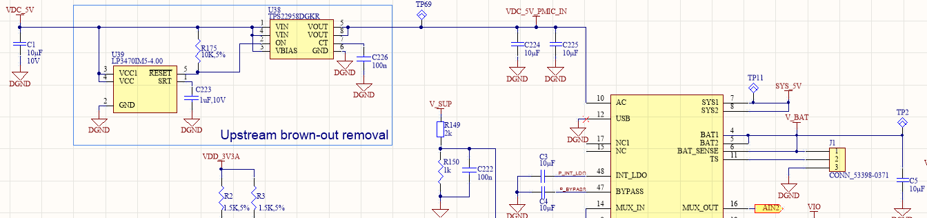
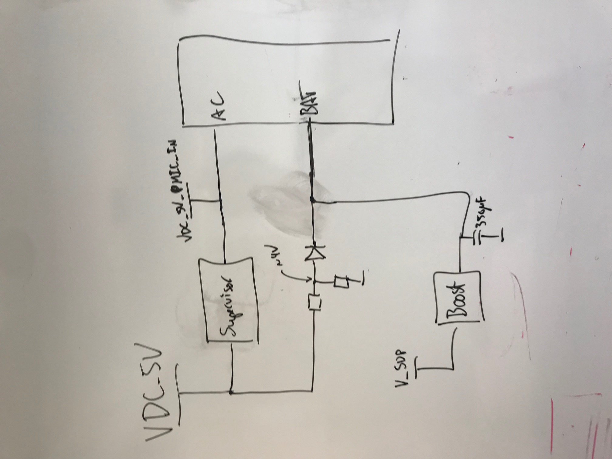
I have designed a board with BBB as a reference design with some additional circuitry around. I am using the TPS65217C with the Solution Circuit Number 3 mentioned in slva901 to avoid lock-up due to input brown-out events. See snip from the schematic below. In additon, V_BAT is connected to the output of a boost converter (with 350uF output capacitance). This boost converter boost the voltage from a supercap up to 5V to provide UPS functionality for some 10s of seconds in case of input power-loss. 

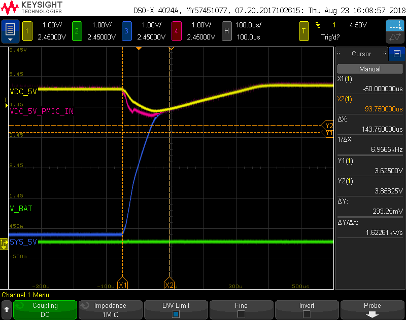
With the supercap discharged, which means that the boost converter connected to BAT is switched off and therefore no voltage applied to BAT pins, I see two different behaviours on power-up: either the board boots successfully after ~2 seconds (delay due to supervisor delay, see slva901), or the board needs an additional attempt (with another 2 seconds delay due to the supervisor) to successfully boot. A successful boot looks as shown below (Yellow trace: "VIN" from slva901, Pink trace: "VIN_PMIC" from slva901, blue trace: voltage on SYS pin, green trace: voltage on BAT pins).

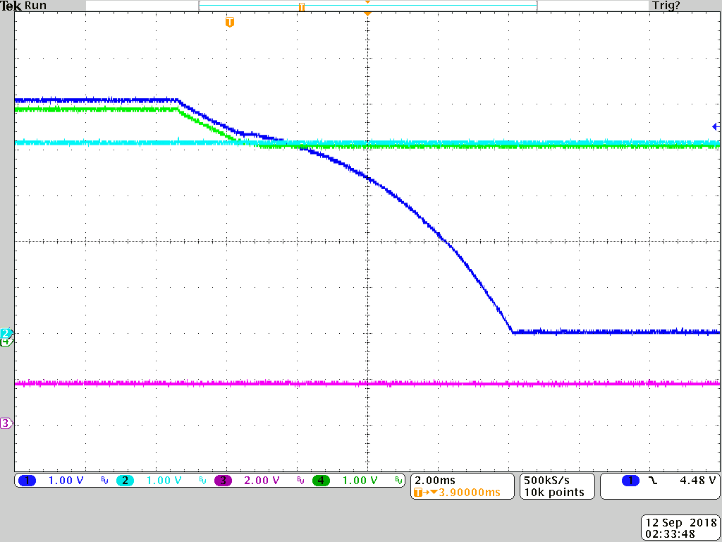
An unsuccessful boot is as shown below. The input voltage on the AC pin on the PMIC (pink trace) shuts down because the voltage VDC_5V dips below 4V which is detected by the supervisor, which in turn shuts down the voltage to the PMIC for another 2 seconds. After those 2 seconds, the board always boots successfully.

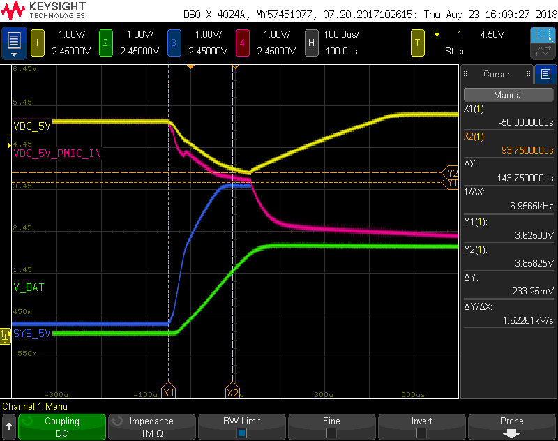
One major difference that can bee seen from the above plots is the voltage on the BAT pin when the SYS voltage is turned on by the PMIC. In the upper plot when the SYS voltage starts to increase the voltage on the BAT pins does not increase, but in the bottom plot the voltage on BAT increases significantly.

For me it seems that the PMIC sometimes during boot connects BAT to either AC or SYS, and sometimes it doesn't. When it does, the additional inrush current to the BAT pin causes the voltage on the input of the PMIC to drop much more, which causes the supervisor on the input of the PMIC to shut down the voltage to the PMIC for another 2 seconds.

Does anyone have any explanation to this? What I particularily don't understand is why the PMIC sometimes decides to charge the BAT pin and sometimes not.

  • Hello and thanks for posting this question on the forum!

    I am glad you were able to use the SLVA901 App Note to build a system that never truly fails, but I see that you are having some difficulty getting your additional circuitry to behave as expected.

    First of all, there is no schematic snip attached to this thread.

    I think the biggest difference between your testing and a normal system with a Li-Ion or LiPo battery is that even when a Li-Ion or LiPo battery is "completely discharged" the voltage on the battery is actually ~2.6-3.3V (depending on chemistry) and if a battery falls below this voltage it is possible the battery will be physically damaged and never work correctly again.

    But in your testing, you are testing a very extreme case when the SuperCap is initially at 0V.
    If you measure the BAT_SENSE pin I think you will see a very subtle difference between the "good" boot case and the "unsuccessful" boot case.

    It is my opinion that testing the SuperCap when it is fully depleted goes outside the operating conditions of the TPS65217 PMIC, and that you should first test to verify the PMIC behaves as expected when the voltage on the SuperCap is only slightly lower then UVLO (3.3 V). Start at 3.2V and work your way down in 100mV steps (3.1V, 3.0V, 2.9V and so on).

    The issue in "unsuccessful" boot occurs because the power supply labeled VDC_5V in your system cannot supply enough current and the voltage droops to an unacceptable level. The problem that causes the reset is the upstream power supply. Added capacitance on the VDC_5V net may help, but it will not solve the "good" boot case in which the SuperCap doesn't charge.

    Although I do not know the details of your circuitry at the BAT pin (boost converter and SuperCap arrangement), I do have one idea that could workaround the issue: install a diode with the anode connected to AC and the cathode connected to BAT. This diode would point in the same direction as the AC power path Q1 FET's body diode and bypass the Q2 FET to the battery that is preventing the voltage from reaching your SuperCap. NOTE: this approach has not been tested and may have an unwanted side effect.

    If you install the diode without fixing the "droop" on VDC_5V, then every attempt to boot the system will be unsuccessful. There are two problems that need to be solved and only one of them is related to the PMIC.
  • Hi and thank you for your reply! Sorry for not attaching the schematic. Here you go: 

    I was perhaps not clear enough in my description of the BAT connection. The supercap is not connected to BAT directly. The supercap is connected to a boost converter that boosts the supercap voltage (which when charged is ~2.6V) to ~5V. The output voltage from the boost converter is connected to BAT. The output of the boost converter has ~350uF output capacitance connected to it. This is the capacitance that the BAT pins "see". Before the supercap reaches ~2.3V the output from the boost converter is 0V (approximately). This is the case I am testing on now.

    I don't want the supercap or boost converter to receive any voltage from the PMIC. The currect flow should only be from the boost converter to the BAT pin, and not the other way around. What I don't understand is why the voltage at the BAT pin sometimes start to increase when SYS is starting, as shown in the bottom plot.

  • Hi again,

    I did some more testing and found a solution that seems to work. As you mentioned, running the BAT pins at 0V (which is the case in my design before the supercap has reached high enough voltage to start the boost converter) might be outside spec for the PMIC. I then figured I could try to sum a voltage to V_BAT before the boost converter is running, ensuring that the voltage at the BAT pins are higher than UVLO at all times when voltage is applied to the AC pin. The voltage to V_BAT is drawn from "VDC_5V", which due to the supervisor is high 2 seconds before "VDC_5V_PMIC_IN", and therefore the voltage at the BAT pin is high before 5V (VDC_5V_PMIC_IN) is applied to the AC pins.

    The summation voltage is divided from 5V to ~4V with a resistor divider. The resistor divider must be low enough impedance so the capacitors (~350uF) on the boost converter output are charged to ~4V before the 2 seconds have passed. See sketch below:

    With this solution I don't see the behaviour that I saw earlier with V_BAT drawing in-rush current at start-up, and the board seems to boot successfully each time. This seems to work because we are now "tricking" the PMIC to believe that a battery is connected to the BAT pins.

    What do you think about this solution? Are there any pitfalls that I haven't considered? Thank you for your time!

  • Hi,

    I noticed in your schematic that the TS pin is not tied to GND through a 10kOhm resistor. In your testing, were you able to deliver current from the SuperCap to the SYS pin when AC is removed? Technically, a floating TS pin means no battery is present, but it is possible the VUVLO detection of the Power Path is allowing current flow in the direction of BAT to SYS. If you notice the current is very limited in this case, it is because current is flowing through the body diode of the Q2 FET from BAT to SYS.

    In your whiteboard drawing, are "VDC_5V_PMIC_IN" and "VSUP" the same net? If not, where does "VSUP" come from?

    Either way, you need to make sure that current will flow in the correct direction from the BAT pin to the SYS pin using the SuperCap when the AC supply is removed, while avoiding the fast-charge region. The following 3 sections of the datasheet show you the regions you need to avoid:

    8.3.9.1 Shorted or Absent Battery (VBAT < 1.5 V), where 1.5V = VBAT(SC), the short-circuit voltage threshold at the BAT pin
    8.3.9.2 Dead Battery (1.5 V < VBAT < VUVLO), where VUVLO = 3.3V by default
    8.6.7 Charger Configuration Register 2 (CHGCONFIG2), VOREG[1:0] = 00b by default, setting the max charging voltage to 4.1V
    As a result, VUVLO < VBAT < VOREG is the fast-charge region and should also be avoided.

    Otherwise, my only concern would be the leakage current through the "resistor divider with low impedance". If this is acceptable in your system and the resistors are not getting hot, then I am OK with your implementation.
  • Hi and thank you for your reply.

    V_SUP is the supercap voltage, which is boosted to 5V and applied to BAT when the supercap is charged. I am successfully delivering power from the supercap to the sys pin when AC is removed. The current from the BAT pin to the SYS pin is then ~700mA.

    Is it important to avoid the fast-charge region if the charger is disabled (through the CH_EN bit)? Do you still think I should connect TS through a 10k resistor to GND? What change of behaviour should I expect from the PMIC if I do this?

  • As long as the current isn't going from AC to BAT (the un-wanted direction in your system), then your existing circuit is acceptable.

    My concern was only that you may not be able to draw the high current (~700mA) when VBAT>VUVLO but TS == floating. Since you have measured the current, it seems TS is not required for the unidirectional flow of current from BAT to SYS.

    As the BATTEMP bit in CHGCONFIG0 indicates, "NOTE: This bit does not indicate that the battery temperature is within the valid range for charging." It simply means that it did not detect an NTC at the TS pin. As a result, you should not need to change your TS pin termination.

    Setting CHG_EN to 0b manually via I2C only ensures that charging will not occur after a successful boot. Your primary issue was during boot (power-on), when CHG_EN is set to 1b by default. If your system boots successfully every time using the work-around, this is a non-issue.
  • Hi and thank you for your reply! My system has been working stable now thorugh several scenarios so I am very happy with that.

    One last question: the data sheet states that there is a power deglitch time associated with AC or USB voltage increasing that is 22.5ms. Is there also a deglitch time with VBAT increasing? If, say the AC pin dropped down to the same voltage as on the BAT pins, how long will it take for the PMIC to detect this and switch over from powering SYS from AC to powering SYS from BAT? As an example, if the AC voltage dropped to be equal to BAT for 10ms, before increasing again to be higher than BAT (more than 190mV), will the PMIC switch over to use BAT for a short while before being powered from AC again, or will this be deglitched?

  • The "Power detected deglitch" time, tDG(DT), of 22.5ms that you mentioned says it is only for AC or USB voltage increasing. The Power Path is intended to work such that AC, USB, and BAT hand-off is smooth and SYS is always powered when one of the supplies goes away but a different power supply is still available and above the UVLO threshold.

    To provide a good answer, I would need to know the absolute value of the voltage on BAT. The entire Power Path switching is relative to the absolute value of VBAT. And when AC drops, how far does it drop? The exact values are important to providing a definitive answer.

    Around the UVLO threshold, the hand-off may not be perfect. This is the reason for the App Note with Solution Circuit #3 in the first place. When VBAT >> VUVLO = 3.3V, the hand-off of the Power Path will be smooth and you will not notice when the AC or USB supply drops.
  • Hi,

    The absolute value of BAT when AC is decreasing is in my case ~4.5V. If AC drops down to 4.5V from 5V, how long does it have to stay there for SYS to switch to being powered from BAT?

  • Hello, 

    I have captured a few scope shots to help explain the AC to BAT hand-off for SYS power more clearly.

    In all of the scope shots, Ch1 = AC, Ch2 = BAT, Ch3 = PGOOD, and Ch4 = SYS. The power supply for AC overshoots the setpoint but this does not have any impact on the test results.

    1) BAT = 4.2V and AC is completely removed (drops to 0V). SYS switches to BAT seamlessly without interruption.

    2) BAT = 4.2V and AC drops to 4.4V. SYS switches to BAT seamlessly without interruption. When AC returns to 5V, the de-glitch time of 22.5ms is applied before SYS returns to AC power.

    3) BAT = 3.4V and AC drops to 1V. SYS switches to BAT seamlessly without interruption. When AC returns to 5V, the de-glitch time of 22.5ms is applied before SYS returns to AC power. Note that the PMIC tries to charge the battery (which is just a power supply) because BAT is below the full charge voltage of 4.2V

    The only time this stops working is when BAT falls below UVLO = 3.3V, which is why App Note SLVA901 was written.

  • Thank you so much for your thorough description. It all seems clear now and the design seems to work good.

    Thanks for your help!