This thread has been locked.

If you have a related question, please click the "Ask a related question" button in the top right corner. The newly created question will be automatically linked to this question.

LP8861-Q1: layout--PGND

Part Number: LP8861-Q1

Hi team,

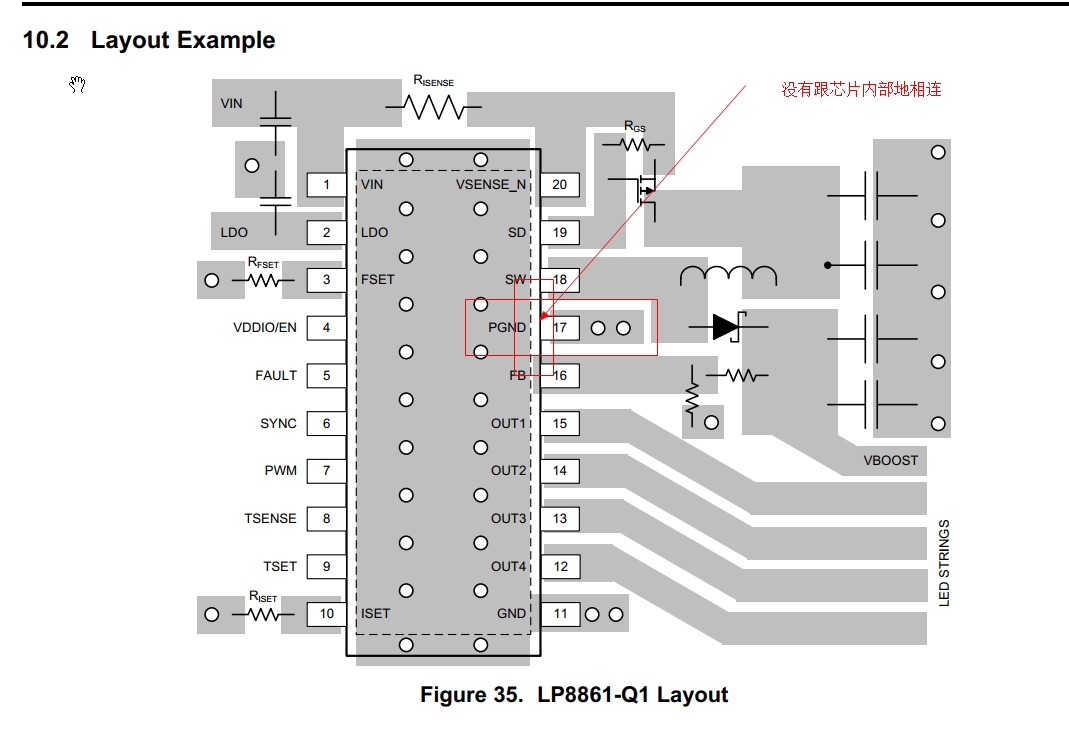
Could you check the recommendation for PGND connection? From the datasheet, it seems PGND is connected to GND through vias, can we connect PGND to GND directly from the top layer?

I checked the evm layout, the PGND is connected with SW. Is that correct?

Dongbao

  • HI Donghao,
    The PGND should connect to GND with a 0R like EVM. It's not suggested to connect to GND directly on top layer. It's suggested to connect to entire PGND layer for better thermal and signal performance. the EVM layout picture seems a little wrong. I will check later. Thanks.
  • Hi Sean,
    Could you share more details about the reason of connecting PGND to the GND layer through vias? I see no difference with the approach of connecting PGND directly to thermal pads beacuse thermal pads still have vias to GND layer.
    Dongbao
  • Hi Dongbao,

    I'm still looking for the original altium file of LP8861-Q1EVM. LP8861-Q1EVM has used separate power and noise-free grounds(with a 0R). Power ground is used for boost converter return current andnoise-free ground for more sensitive signals, like LDO bypass capacitor grounding as well as grounding the GND pin of the device itself. So Isuggested you to tell customers to be careful with layout. Please refer to this application note: www.ti.com/.../snva766.pdf . thanks.

    Sean