This thread has been locked.

If you have a related question, please click the "Ask a related question" button in the top right corner. The newly created question will be automatically linked to this question.

TPS563201: Questions for TPS563201 Additional Feedback Loop Circuits

Part Number: TPS563201

Hi Experts,

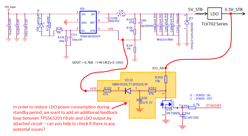
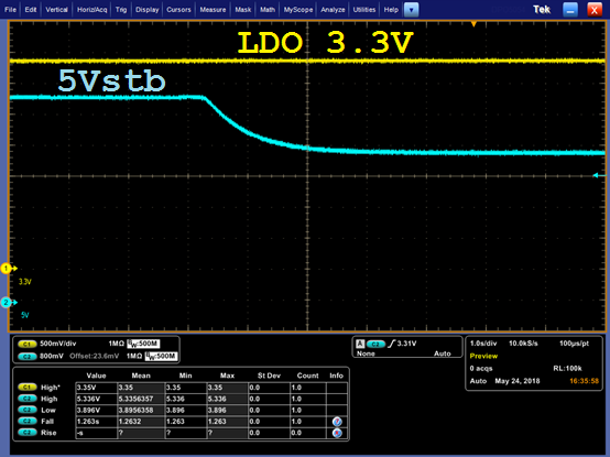
Our customer is using our TPS563201 DC/DC for 12V to 5V application with a post LDO to generate 3.3V standby power, in order to reduce the LDO power consumption during standby period, we created an external circuit as below where during standby period, the 5V_STB will go to around 3.85V from 5V normally. Can you help to check if there is any potential issues for our TPS563201 device? Thanks a lot!

  • Hi Jacky,

    TPS563201 is internal compensation, in order to make sure the loop is stable, please select the L and Cout by referring to datasheet "Table 2. Recommended Component Values". The output capacitance is a litter larger. In addition, the output capacitor is "22uF/6.3V", the rated voltage is too small for 5V output application, as you know there is derating for ceramic capacitor.

    Have you checked that the 5V_STB will drop to 3.85V during standby?

    Shawn
  • Hi Shawn,

    Regarding to the recommended LC configuration, I think that it is followed our recommendation as it is 4*22uF in parallel. Our question is if we can confirm that the additional feedback loop as customer created is fine for our device - can you help to check as you are the experts for these devices. Below is our test waveform for this circuit, it works as we expected for the 5Vstb slow down to around 3.9V when this additional feedback loop kicked in. Thanks.

  • Hi Jacky,

    I think the circuit is feasible, and the waveform looks good.

    Shawn
  • Hi Shawn,
    Thanks for the confirmation.