This thread has been locked.

If you have a related question, please click the "Ask a related question" button in the top right corner. The newly created question will be automatically linked to this question.

TPS65094: VDDQ abnormal react during power sequence G3 to S0

Part Number: TPS65094

Hi, 

A question about VDDQ of TPS650942.

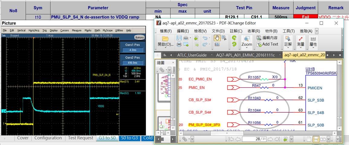
From G3 to S0 , we found VDDQ voltage has abnormal as picture 2.

The different between picture 1 and picture are S3 and S4 signal.

Picture 1,  S3 and S4 from SOC to PMIC

Picture 2, S3 and S4 from SOC to EC to PMIC (abnormal).

I’d like to know which signal may cause VDDQ abnormal. (SLP_S4B or……..)

S3,S4 from SOC to PMIC control. It’s Normal

S3,S4 from SOC to EC to PMIC control . (VDDQ voltage has abnormal)

Please let me know if there are further information needed. Great thanks for your help.

  • There are 3 things I would like to test here.

    1. Are you able to read from the PMIC to see if there is something causing the device to shutdown?
    2. Can you try probing the RSMRSTB pin to see what it is doing during this time?
    3. Can you try probing the SWB1_2 pin to see what it is doing during this time?

    I ask this because VDDQ should turn on about 4ms after SLP_S4B goes high, and here it looks like it turns on beforehand, turns off, then goes high about 500ms after SLP_S4B goes high. My thought is the device could be shutting down or one of these signals could be affecting the state of VDDQ.

    Thank you,
    Nick