This thread has been locked.

If you have a related question, please click the "Ask a related question" button in the top right corner. The newly created question will be automatically linked to this question.

LM3445: AN2069 Dimmer Circuit not Working

Part Number: LM3445

Dear All,

Good day !

I am new to TI family,

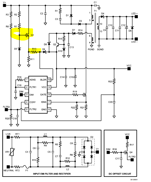
I am working with led dimmer part  for my product( Home Automation System). For this i adopted a application note( AN2069) using silicon LM3445M driver. I designed tyhe dimmer for 8W as mentioned in the application note. I am facing a problem with this application note (R13(33E) and Q1(Part No:-FQT1N60CTF_WS) components are getting failure every time.PFA bellow.

Input voltage :- 150-230V Ac.

  • Nanda,

    Q1 is the FET that provides the initial startup regulator for the device VCC. In addition, Q1 provides the path for the bleeder circuit which is trying to keep the triac dimmer from turning off inadvertently.

    When in operation, the triac dimmer will cause a very large dV/dt that can potentially damage device Q1 if not controlled. The input filter can be the culprit as the dv/dt can resonate the filter and cause excessive ringing. To solve this, usually the damping circuits (Rs and Cs around the filter) might need to be tuned. You should try removing the input filter on a new board and see if the damage is related to that circuit or not. If not, perhaps your AC source is overshooting the target. Q1 is a 600V device on the BoM (which should be ok with the peak voltage on a 230Vac line).

    In general, these circuits are very difficult to tune and will behave differently depending on what dimmer you have in series. It's always a tradeoff to pass EMI and keep the dimmer from shutting off too early and causing visible flickering.

    -JP
  • Dear James Patterson,
    Thank you for your reply,

    i tried removing the input EMI filter section. Still I am facing the same problem.
    My project getting delayed due to this issue. Is there any support give locally or remotely from TI.

    Expecting quick reply.
  • Hello Nanda,

    What value is R13 and R11? How are you heatsinking Q1? Do you know if the primary bias is supplying the LM3445 bias? If not then it is being supplied by Q1. Do you have a thermal camera to see if Q1 is getting hot when operating?

    Do you know when these parts are failing? What operating conditions?

    Regards,
  • Hi,

    1) R13 = 33 ohms, 0.25W & R11 =49.9K ohms,0.125W.

    2) We are using the SOT-223 Package so we are not using Heat sinking but we made a extra plane in PCB for heat dissipation.

    3) We don't have thermal Camera .

    4) It is failing for above 100V AC @50Hz 

  • Hello,

    Can you measure the voltage across R13?  Are Q1 and R13 the only parts to fail or does D5 fail or any other parts?  This part has to dissipate power since it is a linear regulator.  At 100V RMS input the average voltage is about 90V  If Vcc is 12V that leaves 78V across Q1.  Every 1 mA of current means 78 mW of power dissipation in Q1.

    If this isn't a failure caused by the design and it is thermal related you can try using a large package MOSFET with a heatsink to see if it works correct.

    Did you design the transformer for this design?  What is the bias voltage when this is running (where Q1 fails)?  How long in operation before Q1 fails?

    Regards,

  • HI ,

    Thank you for your  response 

    I didn't checked the voltage across R13 as soon as supply given even the 100 V ac  R13  and Q1 failed also  sometimes D5 and lm3445  failing  .

    yes as per application note transformer specification Tx is designed and 15V is bias voltage mentioned in specification we didn't measured in  when running.

    as soon power supply given Q1 failed .

    we will try using larger package mosfet.

  • Hello,

    Sorry I didn't notice this before.  Your primary bias winding is connected backward.  The dot is on the wrong side, pin 4 and 6 need to change places.

    Regards,

  • Thank You for Response,

    You mean I want to interchange the pin number 4 & 6 of the transformer ?  do u have working schematic of this , if there pls share that document .

  • Hello,

    I was looking at your schematic an noticed this.  A flyback should have all secondary windings in the same polarity and the primary swapped (looking at the dots).  Using your schematic, when the MOSFET is on pin one is Vin and pin 3 is GND, the primary winding dot is negative.  This is when the energy stores in the transformer core.  When the MOSFET opens the pin 3 becomes positive (the dot).  This is when the energy goes to the load(s), the secondary winding and the primary bias winding.  This means the connection to the diodes should be the dot for both, pin 10 and pin 4.  As you see pin 4 is tied to ground so that is backwards.

    As it is connected on your schematic the primary bias acts like a forward winding.  If the ratio is 4:1 (just an example) and you apply 100 Vrms the primary bias winding will output 100 Vrms/4, this peak voltage is 35V (100V * 1.414 / 4).

    This happens to be one I was working with earlier:   http://www.ti.com/tool/PMP6024

    Look how the transformer dots connect on this.  The outputs should be opposite of the main primary winding.

    Regards,