This thread has been locked.

If you have a related question, please click the "Ask a related question" button in the top right corner. The newly created question will be automatically linked to this question.

UCC28700: UCC28700 VDS abnormal waveform

Part Number: UCC28700

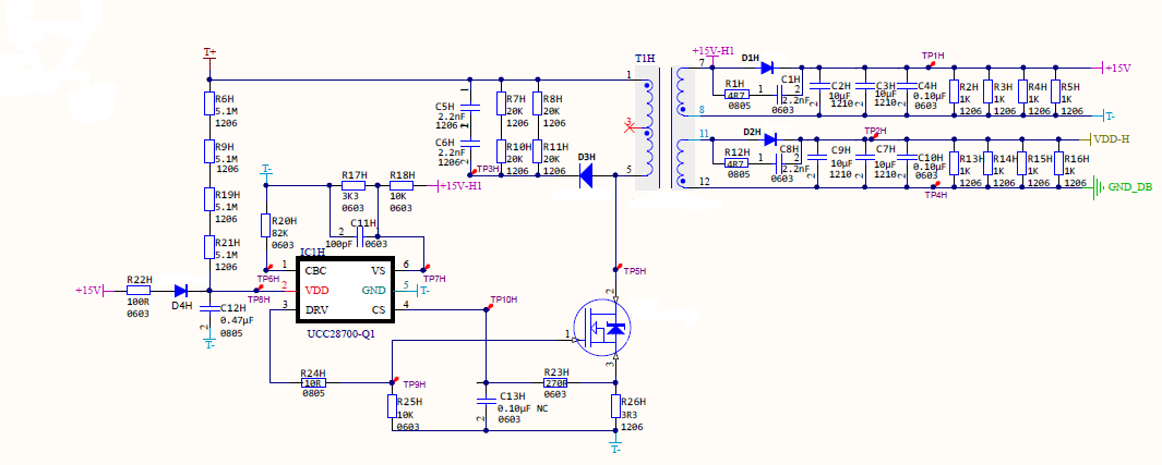
The main parameters of the transformer: the primary side inductance is 1.2mH, and the original secondary side ratio is 3.6:1.

It is found that the VDS waveform of the primary MOS is still shaking, and the waveforms of each cycle are different.

Could you help check?

Thanks

  • Hello Junlong,

    The VS pin regulation voltage should be set to 4.05V (electrical table), the resistor divider is set to the wrong level.

    Please share the whole system spec ie. Input range, Vout, Pout, Fsw etc. to review your design.

    Regards,

    Sonal

  • Thanks Sonal.

    Hello Junlong,

    As Sonal mentioned, Can you provide more information about this design , what the voltage of VDD_H and the load current spec.?
    How about the turn ratios of transformer Np:Ns:Na (Pin1-5:Pin11-12:Pin7-8) ?

    Avoiding place a filter capacitor(C11H) on VS pin since it will impact accurate sensing waveform on this pin. and the value of 100pF is a little large.
    R25H is not necessary on here since it will impact the turn on rate of FET , and there is a internal 200Kohm pull down resistor.

    Can you share more details about the waveform you captured , such as what is the input voltage and output load , Fsw ?
    Please note that the controller will entry valley switching for reducing EMI , it means the switching frequency is always with minor change.
    As you can see the turn on point always at the valley , that means the control principle was correct.

    Thanks.
  • Fixed a minor mistake.

    Please note that the controller will entry valley skipping mode for reducing EMI .

    Thanks
  • The input range of the system is DC60V~DC500V, the one output is 15V 150mA, another output is 10V 100mA.

  • Is it possible to understand that frequency change is a function of the chip itself, is it a normal phenomenon?
  • Hi Jaden,

    a more serious problem, the 15V voltage will drop to 9V when the output is full, 10V will fall to 6V, but in the case of half load, the output 15V and 10V are stable, how to adjust?
  • Hi Junlong,

    There are total 1.3W power consumption on your output dummy load. so you have to consider this load when you calculate the Rcs(R26H) resisitor
    Based on my calculation , Rcs should be less than 1.56ohm . you can find the calculation formula on DS page 21th.
    So please change you Rcs resistor value firstly.

    One more question: we you found this issue , how about the input voltage and switching frequency?

    The frequency minor variation is normal phenomenon.
    Thanks.