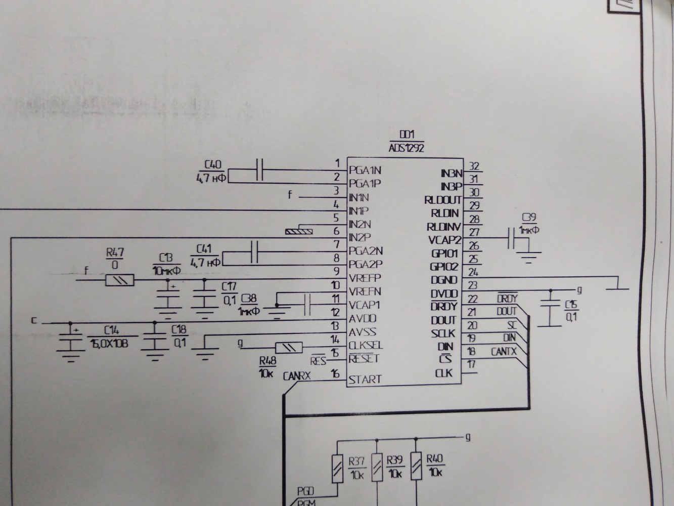
Hello. I use the ADC ADS1292 in my project. AVDD = 5V, DVDD = 3.3V, IN2P = 200mV. I configured this ADC first according to the "Quick Start" instruction in the datasheet. I get instead of real values of 0x7FFFFF on both channels, the status bit is correct - 0xС00000. I tried to turn on the calibration - the result is the same. Here is the detailed code for initialization of this ADC in MPLAB x IDE:
#define ADC_REG_DEVID 0x00
#define ADC_REG_CONFIG1 0x01
#define ADC_REG_CONFIG2 0x02
#define ADC_REG_LOFF 0x03
#define ADC_REG_CH1SET 0x04
#define ADC_REG_CH2SET 0x05
#define ADC_REG_RLD_SENS 0x06
#define ADC_REG_LOFF_SENS 0x07
#define ADC_REG_LOFF_STAT 0x08
#define ADC_REG_RESP1 0x09
#define ADC_REG_RESP2 0x0A
#define ADC_REG_GPIO 0x0B

#define ADC_CMD_START 0x08
#define ADC_CMD_RDATAC 0x10
#define ADC_CMD_SDATAC 0x11
#define ADC_CMD_STOP 0x0A
#define ADC_CMD_OFFSETCAL 0x1A
#define ADC_CMD_RREG 0x20
#define ADC_CMD_WREG 0x40


LATBbits.LATB2 = 0;      // pin CS to low
LATBbits.LATB3 = 0;       // pin START to high

ADC_RESET = 0;
Delay10TCYx(9); // delay 8.14 μs
ADC_RESET = 1;
Delay10KTCYx(256); // delay 460 ms
Delay10KTCYx(256);

ADC_Stop();
ADC_SetConfig();
ADC_Start();

void ADC_SetConfig (void) {
// stop continuous read mode
ADC_SendCommand(ADC_CMD_SDATAC);

// set continuous conversion mode
// set sample rate to 125sps
ADC_WriteRegister(ADC_REG_CONFIG1, 0b00000000);

// enable internal reference
// set internal reference to 2.42v
ADC_WriteRegister(ADC_REG_CONFIG2, 0b10100000);

// enable channel 1
// gain x1
// normal electrode input
ADC_WriteRegister(ADC_REG_CH1SET, 0b00010000);

// enable channel 2
// gain x12
// normal electrode input
ADC_WriteRegister(ADC_REG_CH2SET, 0b01100000);

// RLDREF signal (AVDD – AVSS) / 2 generated internally
// calibration on
ADC_WriteRegister(ADC_REG_RESP2, 0x83);

// enable RLD buffer
ADC_WriteRegister(ADC_REG_RLD_SENS, 0x20);

// init the remaining registers with default values
ADC_WriteRegister(ADC_REG_LOFF, 0x10);
ADC_WriteRegister(ADC_REG_LOFF_SENS, 0x00);
ADC_WriteRegister(ADC_REG_LOFF_STAT, 0b00011111);
ADC_WriteRegister(ADC_REG_RESP1, 0x02);
ADC_WriteRegister(ADC_REG_GPIO, 0x00);

ADC_SendCommand(ADC_CMD_OFFSETCAL);

}

void ADC_SendCommand(BYTE command) {

ADC_CS = 0;
spi_send_b(command);
ADC_CS = 1;

}


void ADC_WriteRegister(BYTE address, BYTE value) {

ADC_CS = 0;
// writecode + address
spi_send_b(ADC_CMD_WREG | address);
// write 1 register
spi_send_b(0);
// write register value
spi_send_b(value);
ADC_CS = 1;

}

// Channel data(24 status bits + 24 bits ? 2 channels) = 72 bits

void ADC_UpdateChannelData(void) {

BYTE i, j, tmp;
ADC_CS = 0;
// read 3 byte status register (1100 + LOFF_STAT[4:0] + GPIO[1:0] + 13 '0's)
tmp = spi_rcv_b();
tmp = spi_rcv_b();
tmp = spi_rcv_b();


for(i = 0; i < 2; i++)

{
channelData[i] = 0;
// read 24 bits of channel data in 3 byte chunks
for(j = 0; j < 3; j++)
{
tmp = spi_rcv_b();
channelData[i] = ((channelData[i]) << 8) | tmp;
}
// convert 3 byte 2's complement to 4 byte 2's complement
if((channelData[i] >> 23) == 1)
{
channelData[i] |= 0xFF000000;
}
else
{
channelData[i] &= 0x00FFFFFF;
}
}
ADC_CS = 1;

}

void adc_ready_interrupt (void)
{
     INTCON3bits.INT1IF = 0; // сброс флага прерывания
     ADC_UpdateChannelData();

}
I tried to disable the channels - I got a value of 0 on them, which means that the write commands are executed correctly. I tried to turn on the test mode to get at least some data (in the CH1SET register I chose 0101 = Test signal mode and set 0b10100011 in the CONFIG2 register) - still the same values of 0x7FFFFF. Tell me, please, what could be the problem?