


Other Parts Discussed in Thread: TPS62135
Hi,
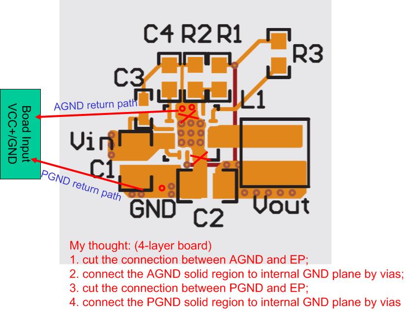
I’m using TI’s DC/DC TPS62130, and have read the paper “Five steps to a great PCB layout for a step-down converter”, in which the idea that handle high-current part and small signal part separately helps me a lot for layout. Now I have a question about the final connection about AGND, PGND and EP-GND:
Can I keep the AGND, EP-GND, PGND clear of each other, on the top plane(main routing plane for the DC/DC chip), and just connect them to the GND plane by independent vias? but doing this, basically they share the same voltage base line and thus the internal circuit of tps62130 can work normally; secondly the AGND return path and PGND return path will un-likely infer each other. (less spike coupled into the small signal circuit in AGND domain?). Could anyone help to check my thought and give any advice?
thanks!
Zhengyun Liu

