Hi team,
I would like to use CSD13302W.
Q1: VDS is12V. What is VDS voltage? Does it mean the VDS voltage cannot be higher 12V for CSD13302W?
Q2: What do the below parameters mean?
td(on) Turn On Delay Time
tr Rise Time
td(off) Turn Off Delay Time
tƒ Fall Time
Would you provide a graph to explain these parameters?
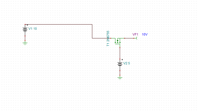
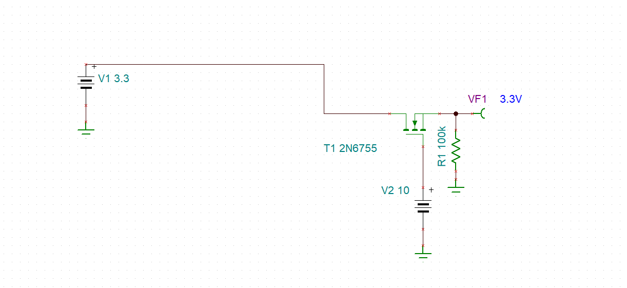
Q3: Can I use NMOS CSD13302W to switch a 3.3V voltage? Like the attach. 2pin is 3.3V/60mA input. 3 pin is 3.3V output. 1pin is controlled by MCU,
If this can be achieved, would you send me a correct circuit or a TINA circuit?