Because of the holidays, TI E2E™ design support forum responses will be delayed from Dec. 25 through Jan. 2. Thank you for your patience.

This thread has been locked.

If you have a related question, please click the "Ask a related question" button in the top right corner. The newly created question will be automatically linked to this question.

LMG1020: Why is input pulse width substantially larger than output pulse width

Part Number: LMG1020

Hello,

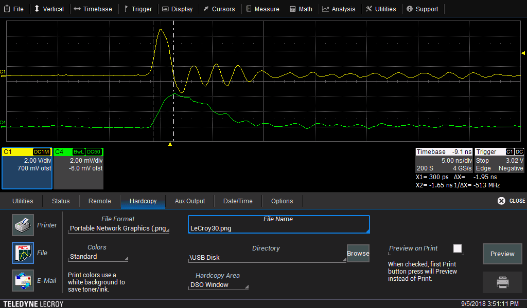
I'm using the LMG1020-EVM board from TI.  I'm testing this because I am planning on using the LMG1020 in a custom diode driver design.  The evm is advertised as a 1nS pulse width capable driver.  Does the 1nS pulse width spec apply to the LMG1020?  I'm seeing that the LMG1020 can produce a pulse close to 1nS, but I don't see anything close to 1nS at the output of the GaN FET.  By output I mean the "current" waveform through the diode.  The Green trace was produced by a ThorLabs DET080C detector.  The yellow trace is the gate of the EPC GaN FET on the board.

My test setup produces a ~2nS pulse at the gate of the GaN fet, but the output is ~10nS.  I've removed the load resistors and placed a diode (OSRAM SPL PL90_3) as the load.  The data sheet is attached.

SPL PL90_3_EN.pdf

I've cut the legs as short as I can and attached it in the most optimized way I could (short leads, clean solder to pads to eliminate ESL etc..).  I'm driving the diode power (J2) with 30V in this case.  I've noticed that if I increase ONLY the diode power the FET output width gets substantially wider.  For example - going from 30V to 50V at J2 increases the output pulse width by 5 times.  This is when ONLY increasing the diode voltage.  


In summary I have a few questions.

1.  The way TI describes this evm is that it can generate a 1nS pulse width, but does TI mean this 1nS applies to the LMG1020 output only or the performance of the actual GaN FET?

2.  Is it possible to get a 2nS pulse out of this board with an input voltage of ~60V.  The board I believe is rated to 75V so using a fairly high (say 60V) power can you produce a 2nS pulse from the FET?

3.  I noticed the and gate on this dev board/evm is only rated (in the data sheet) to perform at 100Mbits.  This leads me to believe that the and gate can only produce a pulse of 10nS.  Is this correct? It seems like the and gate is not capable of producing a 1nS pulse.  

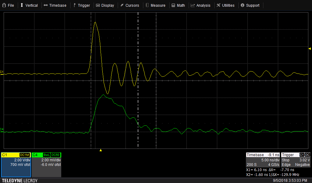
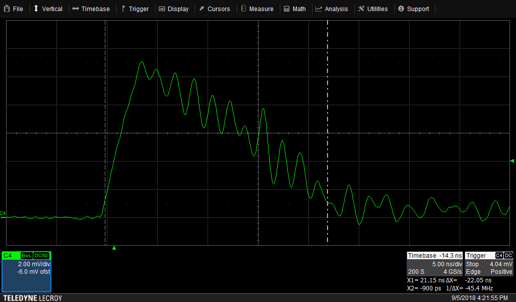
4. The below screenshot shows shows the detector response when I increased the diode voltage.  There is a lot of oscillation here.  The below screenshot shows the response from the ThorLabs DET080C just like the above screen shot mentioned above.  This is strictly an optical measurement.  For diode driving purposes using this evm is this a common electrical ringing?  

5.  Why does the FET look like it turns on faster than it turns off?

  • Hello Robbie,

    I have assigned this thread to the appropriate contact and they will get back to you soon.

    Regards,
    Mateo
  • Thank you - I am in need of support on this.

    I believe my problem may be due to ringing on the gate of my GaN FET.  I noticed the LMG1020 evm dev board ships with 0R resistors for OUTH and OUTL, but the datasheet recommends 2 ohms.  I'm thinking this may be part of my problem.

  • Hi Robbie,

    Thanks for asking about LMG1020, and sorry for the late reply.
    The EVM UG shows 1.5ns pulses seen on the gate of EPC2019 at 30V. It should be possible to do this at 60V.
    The hardest part about getting the short pulses is the parasitic effect in the output loop.  Its also important to make sure 1-2ns pulse is being applied to the input pins on LMG1020. The 2 ohm gate resistor will only slow down the pulse but may help with ringing. The reason for all the ringing is during turn off the current stored in the stray inductance has no where to go and resonates with Coss of the fet.  Turn on there is no ring since there is no current flowing which the diode is soft switched. To achieve less than 2ns gate pulses (50% rise to 50%fall) can you confirm the input pulses are 1-2ns as described in section 7.1 of EVM UG? also can you confirm what is your 20% to 80% rise time?

    Thanks,

  • Jeffery,

    Thank you very much for the response. I will get some more test data this week to address your question. The pulse width above in yellow is the gate pulse. It is pretty short and ~2nS, but I will do further testing as soon as I can.

    What about the turn off time? It looks like there is a really long turn off time. The oscillations (green trace) look like they are riding on a slope which seems like a slop created by the FET turning off slow. Do you have any comment on this? Ideally the FET turns on and off quickly so there isn't smearing in the optical domain.
  • Hi Robbie,

    Thanks! Thats correct! the ringing is riding on the falling slope of the GAN gate. The falling edge is slower than the rising edge due to the asymmetrical drive current of LMG1020. This driver does so well with the rise times needed for fast pulses and achieving a nice pulse shape where the falling edge is permitted to be slower to allow a softer turn off. When turning off a fet there can be current still flowing and if that current suddenly stops the parasitic inductance is excited and will soon see Coss and resonate. To achieve a faster turn off, reduce and gate resistance so the peak sink drive current is not impeded. The shape the laser pulse is also dependent on the laser diode leads and contributes to more loop inductance in the power train which can widen rise and fall times.

    Thanks,
  • How would I reduce the gate resistance?  I'm using the LMG1020 EVM.

  • With R1 and R2 gate resistors. However these should be 0ohm out of the box.
  • Correct. They are 0R right now so I am wondering if there is anything else I can do to bring the turn off time down.
  • Reduce laser diode lead length to reduce parasitic inductance or use a smaller gate charge GAN.

  • What sensor / test equipment did TI use to measure the pulse width during the 1.5nS operation of this dev board?
    1. There is no electrical way to measure the electrical pulse width correct?
    2. Did TI measure the pulse width optically?
    3. If so what detector did you use?
    4. What is the best way to measure the pulse width and peak power of the pulse?
    5. Did TI have all the caps loaded in the diode voltage capacitor bank for the 1.5nS output test pulse?
  • Hi Robbie,

    Thanks for the follow up,

    1) what pulse width are you referring to GAN gate? GAN peak current pulse?
    2) Conversion from light back to electrical signal means to measure the intensity of the pulse captured by the optical receiver this is done using a half power pulse width method using a optical power meter similar to Thorlabs PDA150A.
    3) the optical reciever used is Thorlabs DET08C (8 GHz BW)
    4) peak power of the pulse can be seen though a scaling of the area under the half power pulse width of the pulse this is equal to the energy measured by the meter
    5) All the caps were powered and had voltage before the laser was turned on

    Basically the caps dump the energy into the diode (we want to know the peak fet current as well).
    There are two indirect methods to measure current:
    • Create a model to include the parasitic inductances of the components, connections, and PCB traces.
    • Measure the power from the from the light pulses generated by the laser.
    The diode outputs light thats detected by DET08C in order to observe a change in the peak amplitude of the light pulse.
    This amplitude which is proportional to the light power but not WRT energy/time dimension
    Therefore the PDA150A is used to measure the full width at half maximum (FWHM) where the power is at least half the max - this is the area or energy of the pulse as measured by the light meter
    Next find the peak of the (FWHM) for the corresponding equivalent area
    Finally Extrapolate the area under the curve with the peak (between the measured power and calculated peak power of the light pulse)
    All this info can be found on page 13-19 of the TIDA www.ti.com/.../tidue52.pdf
    Does this make sense? let me know what step is not clear.
    Thanks,
  • hello

    I am reviewing lmg1020 evm board as well. I have questions above your post.

    Plz let me know how much laser peak current or peak power is? when you test lmg1020 evm using OSRAM SPL PL90_3.

    As lmg evm UG  mentioned , can you get 50 Apk at 2ns (pulse width)?

    Did you improve long falling time ? How about ringing  , when gate resister change to 2ohm.

    thank you.

  • Hi Choi,

    Thanks for the follow up,

    The EVM UG doesnt mention the tested peak current however the TIDA does in fig 3 and 13

    Let me check if we tested with PL90_3 and ill update you. I just ordered this LD and hope to test this out for myself as well.

    The ringing should get better with any gate resistance. The fall time is dependent on the drain current since Id charges Coss during turn off.

    Thanks,

  • Hi Choi,

    we never tested PL90_3 however you should be able to achieve similar performance.

    Thanks,