This thread has been locked.

If you have a related question, please click the "Ask a related question" button in the top right corner. The newly created question will be automatically linked to this question.

UCC27712: No HS output

Part Number: UCC27712

Hi,

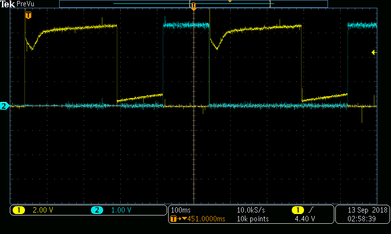
I'm sending 3.3V pulses (@ approx 4Hz) to the HI of the UCC27712, but I'm not seeing anything on the HO pin. VDD is 12V. This is occurring on two separate IC's.

Voltage across the bootstrap cap is approx 6V.

Please help. Let me know if you any other information. 

  • Hello Matthew,
    Thank you for the interest in the UCC27712. I will strive to resolve your questions and concerns.
    The 3.3V input signals to HI, or LI is adequate to satisfy the input thresholds of the device.
    The VDD is beyond the minimum recommended range of 10V.
    The 6V on the HB capacitor however is below the HB-HS UVLO turn on threshold. So the HO output will be disabled.
    If VDD is 12V and you only have 6V on the bootstrap capacitor the HS pin must be ~5.5V above ground.
    With a bootstrap diode and capacitor, the bootstrap cap is charged from VDD when the HS pin switches to ground. This normally happens when you turn on the LO output and low side MOSFET.
    If you reduce the HS pin voltage closer to ground the HO output will function. But the HS pin needs to switch to ground to recharge the bootstrap capacitance periodically.
    Is the driver driving high side and low side FETs in a half bridge configuration?
    Is there any resistance, or other connection from the HS pin to the power train or ground?

    Regards,
    Richard Herring
  • Hi Richard, thanks for your help.
    Yes, the driver is driving a MOSFET half-bridge. When I measured, the midpoint is around 6V from ground.
    There isn’t any other connection between HS to ground.
  • Hello Matthew,

    Thank you for confirming the midpoint of the half bridge which is what I suspected.

    In order for the bootstrap capacitor to fully charge from HB to HS from VDD there needs to be a resistive path from HS to ground. This normally happens when the low side device turns on and HS is pulled close to ground.

    In your case, if there is only HI inputs, and no LI the low side FET will not pull HS to ground to fully charge the boostrap capacitor.

    What load is the MOSFET half bridge driving? Normally there will be a transformer or inductor connected to the MOSFET half bridge which provides a current path from HS to ground. If you are only testing the driver and MOSFET half bridge with no power train connection, you can add a resistance from HS to ground which will allow the bootstrap capacitor to charge. In this case the HO output should operate.

    Regards,

    Richard Herring

  • Hi Richard,

    I think what I'll do is have the microcontroller hold the LS switch closed for a short duration, and then it will resume normal operation.

    Previously, I was only testing one output at a time, which is why the bootstrap cap wasn't charging.

    Thanks for all your help!

  • Hi Matthew,
    If this resolves your issue, can you confirm by selecting the green button on the thread. That will help us a lot. If you have more questions you can just open the thread again and post questions.
    Regards
    Richard Herring
  • Hi, I wrote some code where I'm sending alternating LI and HI pulses, with 0.125ms dead time between; the pulse widths are 0.125s.

    When the LS switch turns on, HO is pulled to ground. I hoped this would allow Cboot to charge when the LS is on, but I'm still having the same issue. As soon as the LS switch turns off, HO spikes to the HS switch drain voltage, and then settles quickly to VDD/2.

    Cboot = 270nF

    Rboot = 4.7Ohm

    See attached Figures.

    Fig 1: Yellow = VHO, Blue = LI

    Fig 2: Yellow = LO, Purple = VHB-VHS

    Fig 3: Yellow = HI, Purple = VHB-VHS

  • Sorry, type -
    Fig 1: Yellow = VHS, Blue = LI.
  • After simulation, removing the GS resistor of the HS switch resolved the issue. The resistor was proving an additional discharge path for Cboot.
  • Hello Matthew,
    Thank you for the feedback and scope plots.
    I see that you are running low frequency during your tests, so we need to consider that for your application. Also to get a better idea how to resolve the issue I will ask you for some additional plots to be able to comment on how to resolve the issue.

    Since you are running with long on times for the driver outputs, can you provide the component values for the HB to HS bootstrap capacitor, resistor value of high side MOSFET gate to source resistance (if any), and the VDD capacitance? Also what is the VDD voltage to the UCC27712?
    Refer to the UCC27712 datasheet section 9.2.2 for guidance on selecting the bootstrap capacitance and VDD capacitance. Since the frequency is low, be sure to consider the HB quiescent current as this will discharge the HB-HS capacitor. Also the gate to source resistance will discharge the HB-HS capacitor. So if you have gate to source resistors on the high side FET, you may want to try removing this resistance.

    For the waveforms to determine what is going on with the drive signals, and HB bias can you capture additional plots?
    If you probe HO to ground what you are seeing is the combined voltage of HO-HS and HS to ground. To clarify take some additional plots.
    1) HO, HB, HS, and HI. Take on the same voltage scale with HO, HB and HS with the same ground reference location, that will clarify what each signal is doing with respect to HS.
    2) LO, HO, HB, and HS. With HO, HB, HS same scale and ground reference.
    3) HI, LI, LO, HO

    If is not clear what HS is doing and also HO relative to HS from the scope plots so far. We can resolve the issue with a little more investigation in the details.

    Regards
    Richard Herring
  • Hi Richard, thanks for the input.
    Between removing the GS resistor and increasing the switching frequency, my issue is resolved.