This thread has been locked.

If you have a related question, please click the "Ask a related question" button in the top right corner. The newly created question will be automatically linked to this question.

TPS53318: No operation with load

Part Number: TPS53318

Hi,

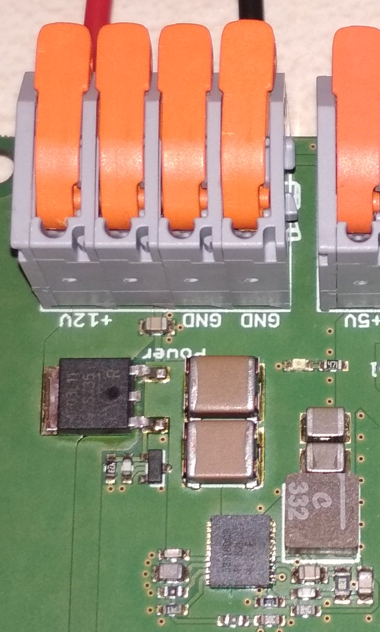
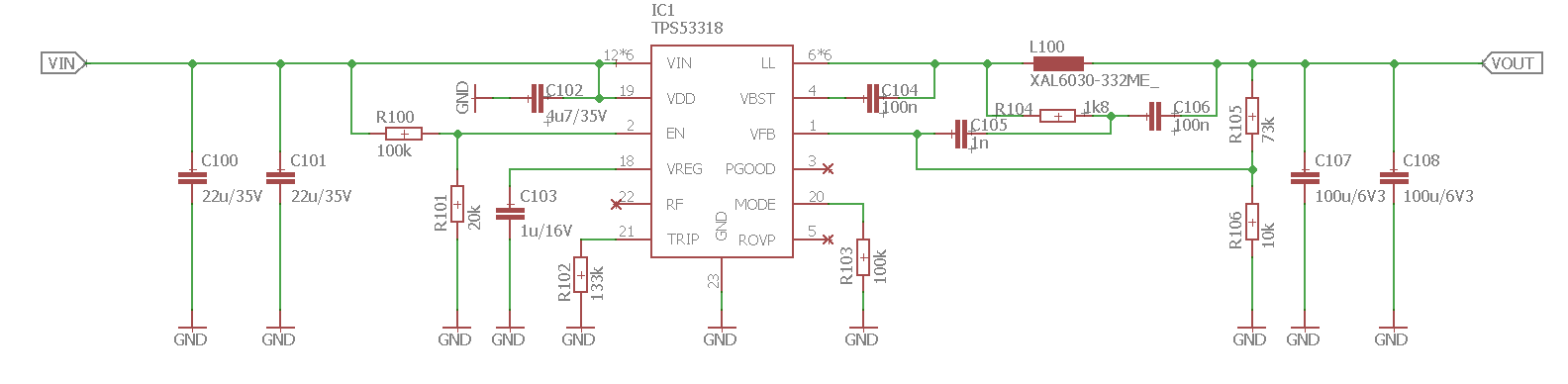
I built a DC/DC converter with the TPS53318 which should work from 12V input and should give me 5V and up to 8A on the output. Here is the schematic:

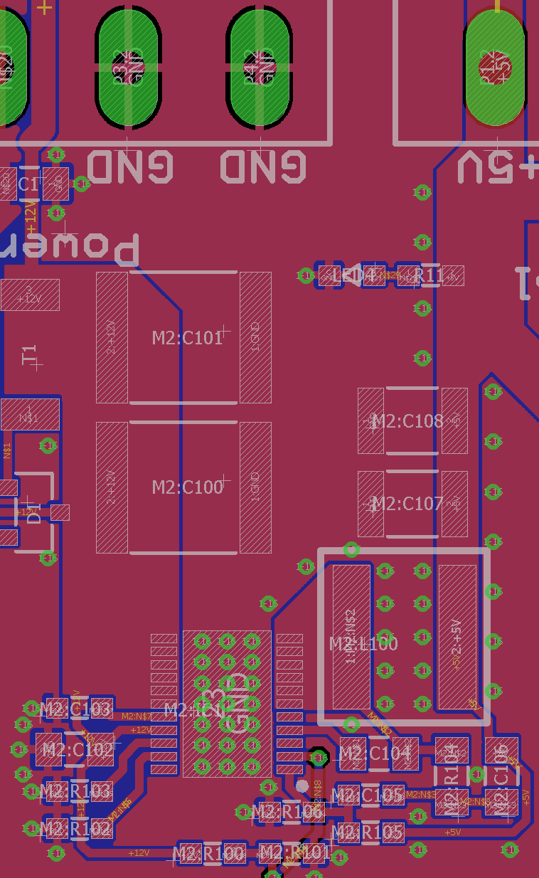
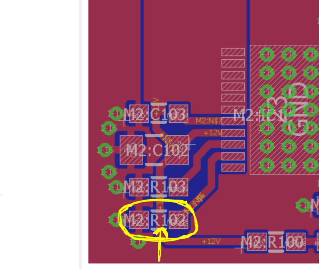
It is based upon a Webench Design which can be found here:

/cfs-file/__key/communityserver-discussions-components-files/196/webench_5F00_design_5F00_3708651_5F00_31_5F00_80219519.pdf

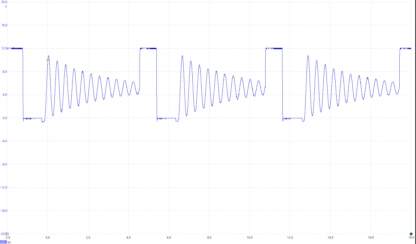
My problem is that the output voltage will by maintained at a light load only. If the output current goes above a few hundred mA, the output voltage collapses. I did some measurements and wonder about the voltage on the power output (pin 6...11, measurement done if output voltage is present):

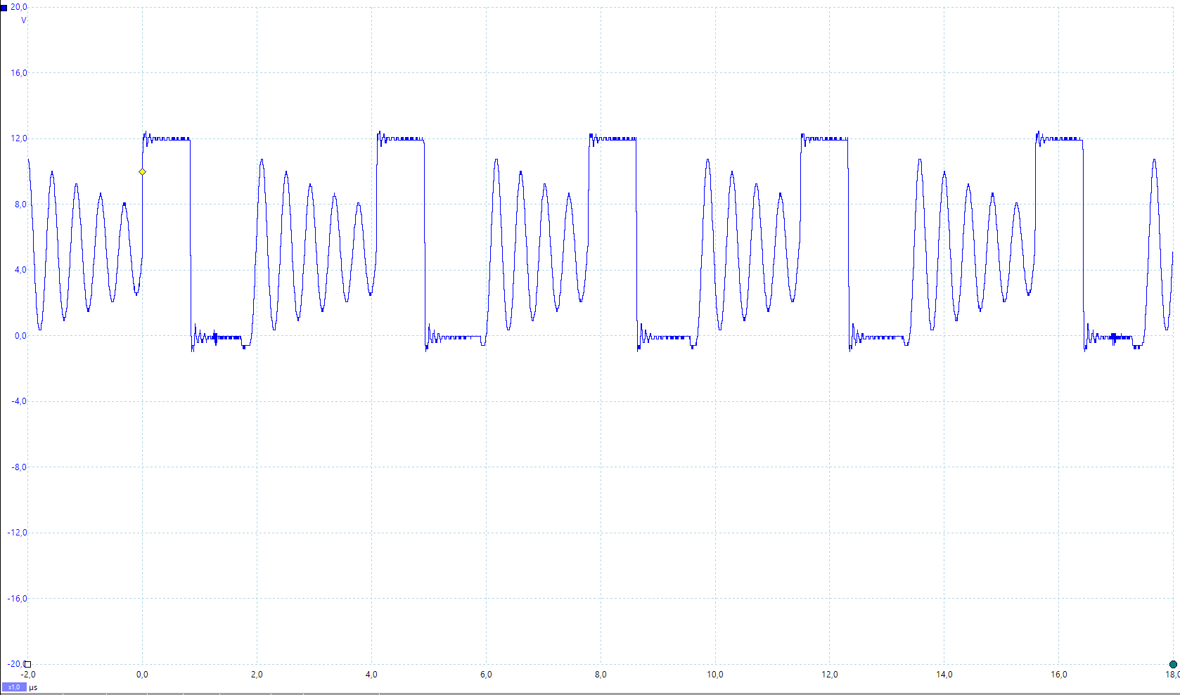
I know how it should look like normally, but I don't know what is happening here. Any hints or ideas?

Thanks in advance for any help!

Best Regards,

Andreas

  • Hi,

    The waveform looks like you are operating in Discontinuous Conduction Mode.
    A couple thing to check:
    1) A noise coupling in to your ripple injection network (R104, C106)
    2) Noise on the current limit TRIP pin
    3) Input capacitor layout in relative to IC.

    Maybe there is something in the layout that affects the IC sensitive node. An EVM layout could be used as a starting point

    Thanks
    -Arief
  • Hi Andreas,

    Just to add to what Arief mentioned, please let us know what your test setup looks like.

    We may be able to help more if we know your probing technique, how your cabling is set up, how connections are being made, etc...

    Thanks,
    Alec
  • Hi,

    thanks for your answers so far. For better understanding, here is a photo of my PCB:

    And a snapshot of the layout:

    As you can see it's a very small piece of circuit. I also tried to keep the sensitive traces very short - very similar to the layout proposal of the datasheet.

    Best Regards,

    Andreas

  • Andreas,

    There are two things that jump at me when looking at your layout:

    1) As Arief mentioned noise on the TRIP pin could cause an issue. R102, the resistor on the TRIP pin has the +12V input signal routed between it's pads. The input signal is going to be a very noisy signal and this has the potential to couple noise onto the TRIP pin.

    2) It looks like you are using a FET on the +12V input signal. Not knowing what you have and have not checked yet, it would be a good idea to ensure the part is getting a constant input supply and there are no issues with the FET, if you have not already done so.

    For quick debug recommendations, to ensure noise from the input supply and/or switch ringing are not issues, you could place a small bypass cap near the Vin pins (0603 0.1uF-1uF). You could also try adding a 3 Ohm boot resistor.

    See this app note for more info on switch node ringing for this part: www.ti.com/.../slua851.pdf

    If you have more waveforms from your debugging could you please share them? This will help us get a better understanding of how the part is behaving, and maybe some insight into why Vout is collapsing. Vin and LL would be very useful, as well as any other signals you could probe.

    Thanks,

    Alec

  • Thanks Alec for your comprehensive answer!

    Regarding the FET at the left hand side: This is just a simple reverse polarity protection. I already tried bridging it, but it doesn't have any effect.

    As recommended, I also added a 100nF cap near the Vin pin - no effect. Further, added the 3 Ohm boot resistor. Here is what I'm getting now at the LL pin (with light load of 23R at 5V):

    I tried to make some AC measurement at Vin and also at the TRIP pin, but I had to realize that I'm just measuring a lot of noise which seems to come from a GND loop together with my PC scope. At least if I'm connecting the both grounds, I'm measuring the same noise after turning the DC/DC off.

    Thanks and Best Regards,

    Andreas

  • Thank you for trying those debugging steps and for the feedback.

    One main point to note, is that this waveform you have sent is normal for the SW node in DCM mode. This waveform is showing the part working correctly, just in DCM.

    Can you please share more waveforms with the part not functioning correctly, when Vout has collapsed. The more waveforms and signals you can capture the more I will be able to see and help.

    Thanks,
    Alec
  • Hi Andreas,

    For the time being I am going to close this question. Please reply to this comment if the above suggestions did not help, and you still need assistance resolving this issue. A reply will open the thread back up, and we can continue to look into it.

    Thanks,
    Alec Heierman
  • Hi Alec,
    thanks for asking again, but I couldn't work anymore at this issue as I had to deliver my project to the customer. For schedule reasons I switched to another circuit. Maybe I should buy an Eval Board the next time ...

    Best Regards,
    Andreas