This thread has been locked.

If you have a related question, please click the "Ask a related question" button in the top right corner. The newly created question will be automatically linked to this question.

TLV62568: The both sides of pins have packaging materials.

Part Number: TLV62568

Dear  All

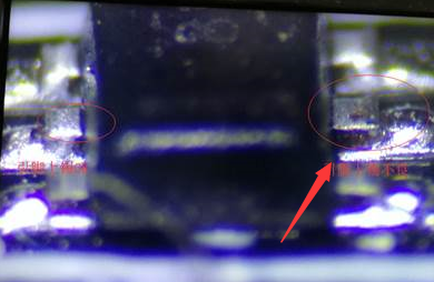
       Look at the below picture, the both sides of pins have  packaging materials. Is it normal ? Does the packaging process require removal of these packaging materials ? Because it will stop to sold the both sides of pin .


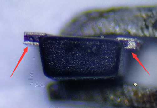
       And the second below picture, the bottom of pins tin plated which are not smooth, the reflection brightness is inconsistentis, is it normal ? why?


  • this looks to me to be the tin coating.
    It is normal is is not shinning, it is MATTE tin
  • Dear Sabrina

    You said the both sides of pin are tin coating ? But why right side is not all black ?

    If the tin coating, it could be sold, right? But in fact ,it can't, look at the below picture.

  • Let me check this with my colleagues and get back to you
  • Can you contact me at my e-mail address: s-ramalingam@ti.com
    I would like t have our packaging expert in the discussion to assess this pictures and find an explanation regarding the packaging material. it will be easier by mail
  • Hi Went Cao,

    meanwhile I could dig  deeper into this case

    1)      Concern: “Packaging material on both sides of the leads” as per customer photo (figure1) below:


    Figure 1: customer photo: arrows pointing to mold flash in the side of the lead


    Assessment: The package material on the sides of the leads is so called “mold flash” and is part of the normal manufacturing process. Mold flash on the side of the lead does not impact quality or reliability of the soldering interface that is established on the bottom side of the lead.


    2)      Concern: “the bottom of pins tin plated which are not smooth, the reflection brightness is inconsistent” as per figure 2 below:


    Figure 2: customer photo showing inconsistencies in the reflection and brightness on the bottom of the lead.


    Assessment: The leads are plated with matte tin (Pure Sn) which is a relatively soft material. The inconsistency in the brightness of the bottom lead side is coming mainly from the insertion of the device into the test socket during the final test operation where the lead is contacted from the bottom side. The appearance of the leads shown in figure 2 above is considered normal and is no concern.


    3)      Concern: Incomplete solder meniscus forming during board level soldering of the device (see figure 3 below). 

    Figure 3:  customer photo of a soldered device showing concerns on soldering and side wetting of the lead.


    Assessment:

    Site A:  Overall soldering looks ok.  Solder meniscus and side wetting  might be limited due to small pad size. Solder meniscus will not rise beyond ~45° angle. If the solder pad on the printed circuit board (PCB) is too narrow the solder will not creep up to the top of the lead. Lead-free solders have a slightly lower capability of creeping up on the side of lead compared to tin-lead-solders (SnxPby) .

    However, this is not a concern as the main soldering interface is on the bottom of the lead.


    Site B:  On site B in the figure 3)  above there are two concerns:

    B1) There is most likely mold flash on the side of the lead preventing the solder to move up on side of the lead.  Assessment: Pls refer to the response above under 1)

    B2) No solder meniscus is forming on lead tip

    Assessment:  The device is plated with tin before the singulation from the lead frame. At the singulation step (trim and form)  the device is cut on the lead tip. Therefore, there is Cu exposed from the lead frame on the lead tip. This is normal part of the process and not a concern. TI cannot guarantee that there is always a solder meniscus forming on the lead tip.

    In order to solve this issue you may consider some key factors influencing the solder wetting on the lead tip. Here are some esxplanations

    a)      Soldering atmosphere: soldering at normal atmosphere (air) can increase Cu oxidation on the lead tip and make it more difficult for the flux to remove the oxide. A change soldering in Nitrogen atmosphere (N2) can improve this.

    b)      Soldering profile: soldering profile. For soldering profile TI is recommends to follow the reflow profile as outlined in the JEDEC standard.

    c)       Careful choice of flux:  the flux capability has a major influence as different flux types  have better or lower capabilities of removing Cu oxide

    Process Control: tight process control for the entire soldering process. Especially time control for the time between solder paste printing and the actual soldering must be kept in order to prevent the flux from drying out which reduces or even eliminates the effectiveness of the flux dramatically.

    I  hope these tips above (a, b and c)  helps you to adjust the assembly process