Dear all,
I was testing IDE_KD bit of FaultMuxRegs register of UCD3138. To test it, I configured DPWM0 and DPWM1. DPWM0 gets its duty from Filter and for DPWM1, CLA is not enabled. Both DPWMs are in normal mode.
DPWM1 duty configurations:
Dpwm1Regs.DPWMPRD.all = 16000;
	Dpwm1Regs.DPWMEV1.all = 0;
	Dpwm1Regs.DPWMEV2.all = 0;
	Dpwm1Regs.DPWMEV3.all = 0;
	Dpwm1Regs.DPWMEV4.all = 16000;
With this configuration, I expect 0% duty cycle and continuous on DPWM1B.

To get duty of DPWM0, I configured Filter out clamp registers as:
            Filter2Regs.FILTEROCLPLO.bit.OUTPUT_CLAMP_LOW = 15520;
            Filter2Regs.FILTEROCLPHI.bit.OUTPUT_CLAMP_HIGH = 15520;

With this configuration, I expect 97% duty cycle.
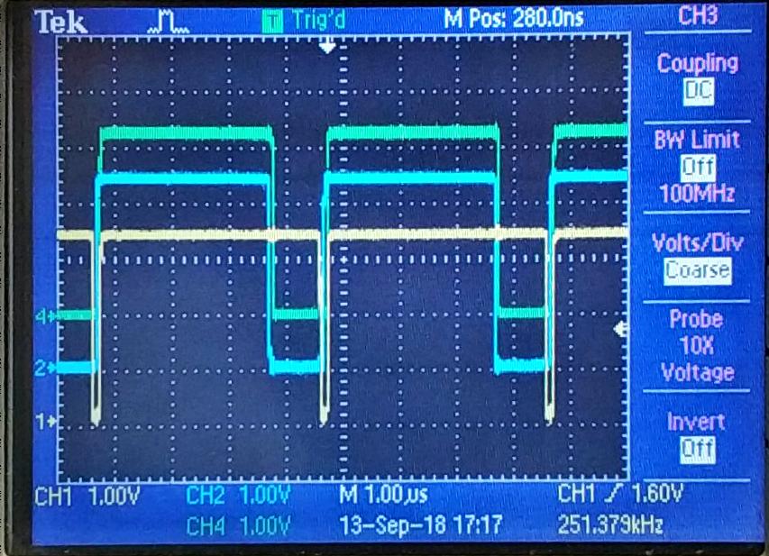
I enabled both IDE for DPWM0 and DPWM1 and I set IDE_KD bit as 400. At the end, I observed the scope screen below where yellow is DPWM0A, blue is DPWM0B and green is DPWM1B.
My questions are:
- With this configurations, DPWM0A and DPWM0B pins are on at the same time which leads to cross conduction of two complementary FETs. Is there any method to eliminate this problem?
- DPWM1A has 0% duty cycle. How is DPWM1B duty calculated without any duty of DPWM1A? The reason why I am asking is this, it is written as "Db is calculated by Da (Filter Duty) times IDE_KD" in Technical Reference manual in page 233.
Thanks in advanced.
Best Regards,
Merih