This thread has been locked.

If you have a related question, please click the "Ask a related question" button in the top right corner. The newly created question will be automatically linked to this question.

LM5088: Inverting Buck-Boost Configuration

Part Number: LM5088
Other Parts Discussed in Thread: LM5085

Team,

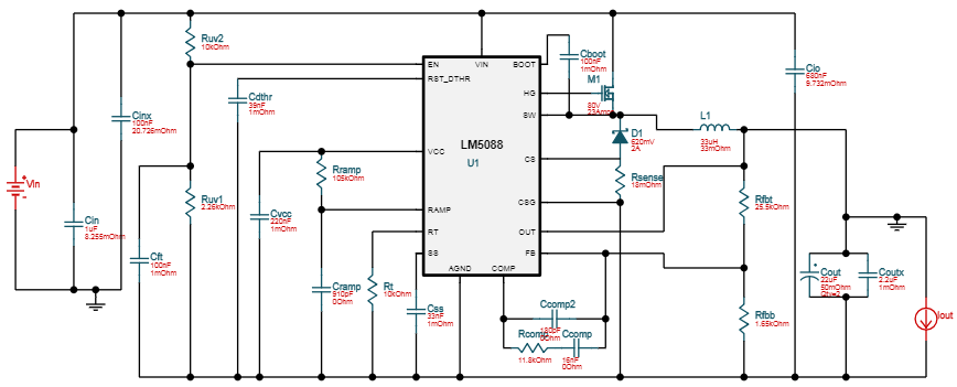
My customer is looking for an inverting buck-boost: 8V-46V input, 20V output @ 1A continuous with 5s spikes up to 5A. I am looking at the LM5088 which seems to have a wide enough Vin to be used in an inverting buck-boost configuration for their specs, but just want to confirm that it would work. Do you see any issues with using this device? If not, can you please recommend a suitable FET and diode?

Thanks,

Antonio

  • A standard inverting buck-boost will not work with the buck controller LM5088, the SW node would swing 20V below GND.
    The P-FET controller LM5085 could be modified for this with the catch diode towards -Uout instead of GND, if you do not connect CS and find a way to get feedback right (mirror?). The FET has to block the sum of Uin+Uout.
    But why not use a dedicated IC?
  • Hi Holmer,

    Please see below for the configuration that I have in mind. The IC would be referenced to the negative output so the SW node should still be within specs. Are there any concerns with this circuit? Webench can't seem to find a suitable FET for a 5A output so I just want to understand any limitations:

    Regards,

    Antonio

  • With the shifted GND the IC should work.

    The worst case is 8V in, with non-ideal components this gives D=0,75, and 5A DC out need 20A during the 25% Off-time to recharge the output cap. Actually it is 15A into the cap and 5A to the output, but you have 20A in Fet and diode. This is probably why Webbench cannot find a Fet.

    Taking the Si7148 (75V/28A/11mR) from the datasheet as an example, allowing 50% more Ron from heating, you get 20A*20A*0,011R*1,5*75% = 5W resistive loss not accounting for switching (guess: 2W).

    Using a monster Fet with just 2mR, gate charge rises to 135nC which means Tr=Tf=90ns at 1,5A gate drive. This means 8W switching loss not accounting for resistive losses.

    A compromise in Fet die size will settle around 3-4W for both, or 7W total. To dissipate 7W, you either screw a TO220 to a heatsink, or use a metal substrate PCB.

    A way out might be to drastically lower switching frequency from 550kHz to say 130kHz to get switching loss down, and go for a small Ron with 2 parallel Fets in the 8mR range to spread the heat over the board. Or go for a single D2PAK with reflow-heatsink, a Polar PAK (aka dual-cool, super-SO8 exposed top...) with a glue-on heatsink. Penalty will be board space and inductor size. Side note: Staying under 150kHz with the fundamental is good for conducted EMI.

    As for the diode, 80-100V in D2PAK (MBRB...) or TO277 (SS..P.. / V..P.. from Vishay) is a good start, the first with solderable heatsink, the latter with metal substrate.

    This is a challenge, unless you design for 1A and rely on thermal mass to survive the 5 seconds. My calculations above for 5A DC are probably overkill, but looking at the transient impedance curves of many parts, 5s is closer to DC than to a pulse load.