This thread has been locked.

If you have a related question, please click the "Ask a related question" button in the top right corner. The newly created question will be automatically linked to this question.

TPS2411: Leakage path from Vdd to A pin?

Part Number: TPS2411

Hello TI,

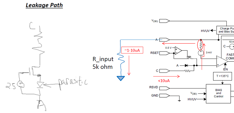
We use TPS2411 as oring circuit to OR BBU (7.2V) and main 12V rail and found there is still around 9.26V at BBU even the TPS2411 is disabled (12V is always presented), confirmed the Gate is 0V.

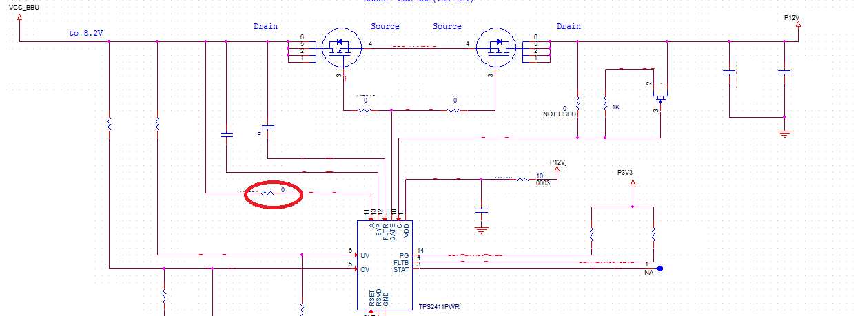
We used to use a jumper (0 ohm) to connect source bus (BBU) to A pin. After we removed the jumper, this leakage voltage is gone.

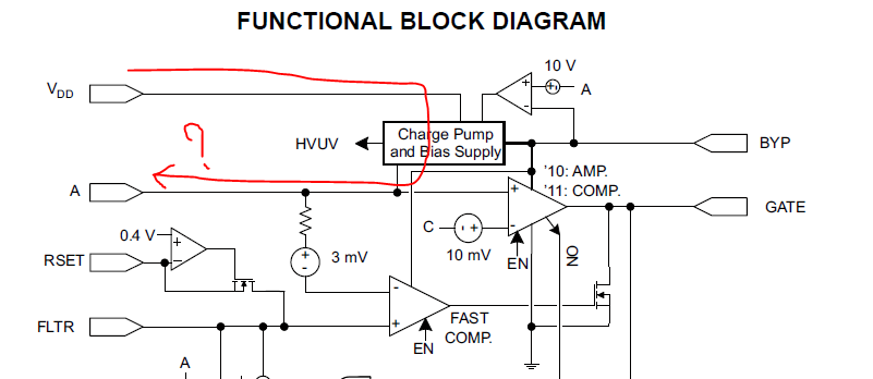
So we want to confirm is there any leakage path from Vdd pin to A pin by Charge Pump and Bias supply section?

Stan.

  • Hello Stan,

    There is leakage from C to A internal to IC. It is shown in the attached PDF document.

    Solution is connect a load on A based on the attached data.

    With 5K at A, I measure 4.6V, --> this means 0.92mA current.

    With 150k at A, I measure 10.0V --> this means 0.066mA current.

    This is consistent with attached measurement from the E2E thread.

    ""

    ""

    1738.1031.TPS241x Leakage Path_Measurements.pdf

    Let me know if this answers your question.

    Regards,

    Kari.

  • Hi Kari,

    Thanks for you reply. The leakage paths are different between two documents. Could you please confirm which one is correct?

    Do you have any ideas regarding the current rating of the parasitic diode and the voltage source?

    Actually this leakage voltage will cause our BBU cannot work properly, we want to use the learning discharge RES to resolve this problem.

    The BBU voltage is 8.2V maximum and the discharge RES is total 16 ohm or 24.7 ohm which is much lower than the discharge RES that you tested with in the document before.

    We want to make sure our learning discharge current won't damage the internal parasitic diode and voltage source.

    BR.

    Stan.

  • Hi Kari,

    By our test result, the learn mode discharge would cause at least 40mA inrush on oring internal.

    Please check if the parasitic diode can accept this inrush.

    BR.

    Stan.

  • Hi Kari,

    Do you have any update regarding the internal inrush capability?

    BR.

    Stan.

  • Hello Stan,

    Sorry for a delay in response.
    I have a question on 50mA of inrush current.
    When the battery is turned from normal operation, can you confirm if this current flows through IC and not the external MOSFET.
    Because MOSFET will intially allow some reverse current (based on MOSFET use) before it turns off.
    Can you please confirm?

    50mA is a little high number to flow through parasitics, we will check on this and get back.


    Regards,
    Kari.
  • Hi Kari,

    It's a estimation based on our design. The BBU learning discharge RES is 25 ohm.

    Do you have any data regarding the current capability of the internal leakage path?

    BR.

    Stan.

  • Hi Kari,

    What if we add the p-ch JFET at A pin same as we did at pinC? Or remove the cap between FLTR and A pin, Any comments?

    BR.

    Stan.

  • Hi Kari,

    Do you have any update/comments regarding the internal current capability of leakage path or my idea?

    Stan.

  • Hi Kari,

    I checked the leakage current during power on/off at C pin side. The leakage inrush current is about 0.68mA. Could you please check is it risky to TPS2411?

    BR.
    Stan.
  • Hi Kari,

    Do you have any update?

    BR.
    Stan.
  • Hi Stan,

    0.68mA of current would not be a problem.

    However, 25 ohm of learning discharge resistance would cause the inrush current through the external MOSFET (MOSFET is initially ON when BBU was turned ON). When BBU is turned off (with discharge resistance of 25ohm), reverse current would flow from C to A through the external MOSFET intially. If this current exceeds the reverse current threshold set, then the MOSFET will be turned OFF.

    Do you see such a scenario?

    We want to confirm if all the inrush current measured flowing through the MOSFET external or the internal to the IC?

    Regards,
    Kari.
  • Hi Kari,

    We do the learning discharge only when the oring controller is disabled. The external MOSFET is B2B connection.

    So we didn't see the scenario that you mentioned. The 0.68mA inrush current that leaked from C(main 12V) to A (BBU) by controller internal path during system power on. I calculated this current by the Vdrop on the resistor(1K) of protection circuit on pin C.

    It's the worst case that even larger than the inrush during learning discharge enabled.

    BR.

    Stan.

  • Hi Stan,

    Thanks for letting us know more about your application.

    0.68mA of current measured through 1kohm resistor is not a concern here.


    Regards,
    Kari.