This thread has been locked.

If you have a related question, please click the "Ask a related question" button in the top right corner. The newly created question will be automatically linked to this question.

TPS53355: The max output current is only 20A

Part Number: TPS53355
Other Parts Discussed in Thread: TPS543C20,

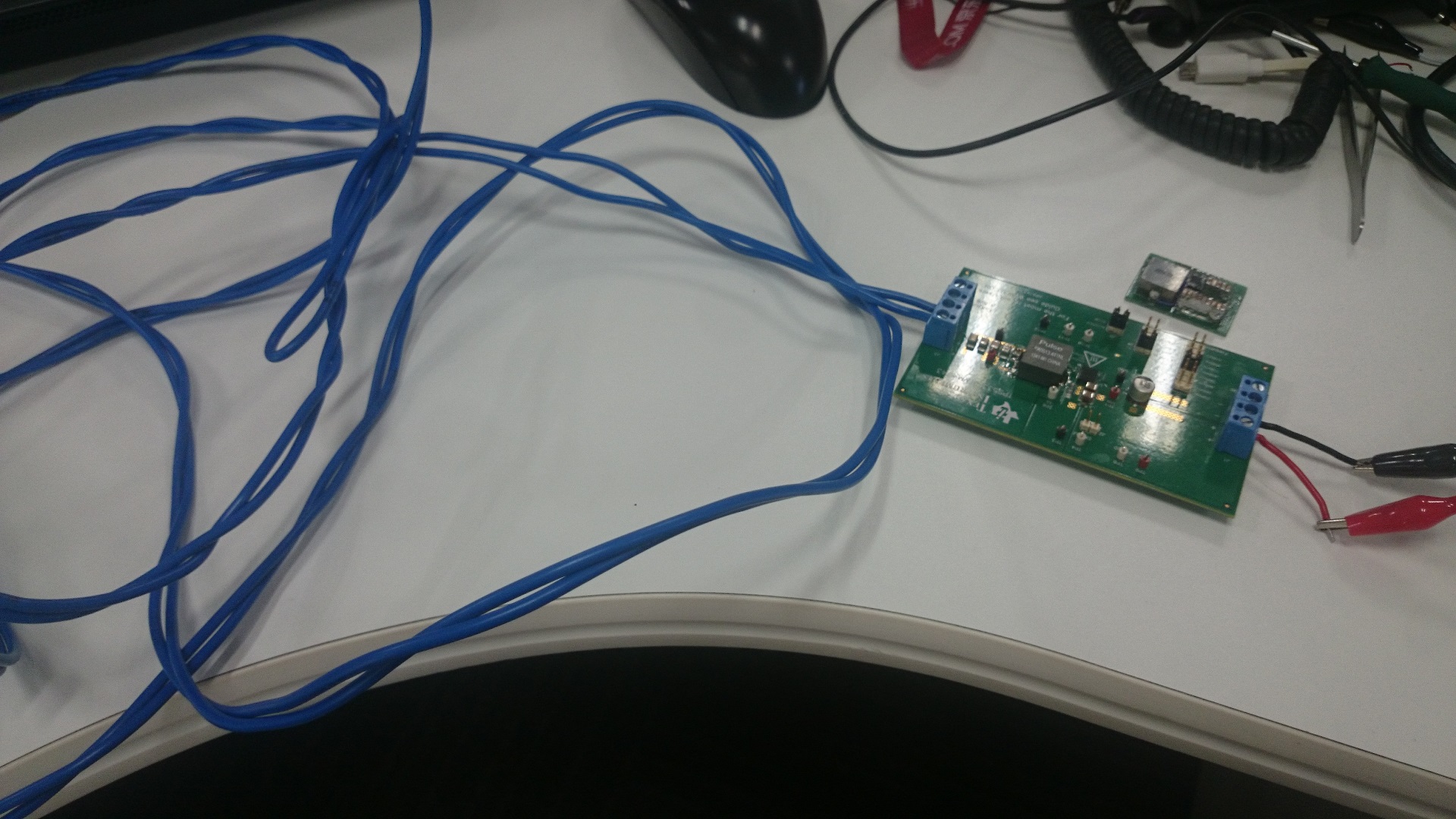
The inductor is MMD-12FD-1R0, its saturation current is 49A. Output ceramic capacitors is 36x10u and input ceramics capacitor  is 20x10u. Input voltage is 15V/10A.

I use 0.1Ohm load and the output current can only achieve about 20A (R7 is 24k). If change the R7 to 39k, the output will soft start up -> shut down ->start up and so on, and the voltage is 0v ->2V->0v and so on .

Change R6 to 300k and change R3 or C6 are useless. When short rf pin (R4), the current will a bit bigger.

A strange thing is that as the temperature increases, the current gradually increases, finally stabilized to 30A。

I also build a TPS543C20 PCBA which use the same inductor and capacitors, it works properly.

  • Modified R6 and R3 and C6, it still doesn't work.
  • Hi user4351886,

    First thing, what is your desire VOUT?  I'm a little confused as why you are changing the R7.  Once you have the VOUT set, please monitor the switch node and vary the load from 0A to 20A to check for stability.  Also, have use tested this configuration on the internal EVM (TPS53355EVM)?  You can order them from the TI store site.

    Thanks,

    Amnat

  • Thank you for your reply.  I will contact TI's agent to try out the TPS53355 demo board。

    The project I am working on is for motor drive. The TPS53355 must provide a maximum current of 30A when turned on, and the output voltage is 5.5V.

    But now the problem is that there is a problem even with the output 3V/30A at startup, so I doubt if the PCB rounting is no very good. The PCB is two layers. One side of is the trace and the ground plane, and the other side is the complete ground plane without any other trace. Ground vias are very dense, including under the IC.

    I don't know if it is because the trace from R7 to the output is a little long.

  • Hi user4351886,

    Thermal should be another concern here.  Your board only have 2 layers and the power consumption is very large here with 30A at 5.5VOUT.  Please look at the datasheet on page 13 for the SOA reference.  The SOA was done on a 6 layer board that can dissipate the heat pretty well. Another concern that I see is the placement of C26 and R3.  These components should be on the bottom side since it can pick up potential noise which can affect your FB to the IC.  This can affect jitter performance or worst, instability issue.  Please let me know the performance once you try this on the internal EVM.

    Thank you.

    Amnat

  • The demo board has been received and the experiment has been done. 
    VOUT has been changed to 3V. Add 0.1 ohm load then power-up is no problem. After power-on, add 0.1 ohm is also no problem.
    As you said, it should be that the feedback line is affected, or the trace from vout to the feedback resistor is too long. The close loop is not stable.
    I will make a new PCB. Rotating the inductor 90 degrees makes vout closer to the feedback pin, separating the noise injection line from the voltage feedback line.
    Thank you! 
  • Hi user4351886,

    Please follow the layout guideline in the datasheet on page 30.  These sensitive component placement is crucial to the successful layout.  Please consider the thermal performance and the SOA limit as well.  I would add at least 2 more layers to be on the save side.  Please place the VDD and VREG by pass capacitors close to the pins.  I can help you do a quick review on your layout before you GERBER.  You can send it to me directly.

    Thanks,

    Amnat

  • Thermal is not a problem. The starting current of the motor may be 30A, but the working current is about 5A and the maximum is no more than 10A(short time). The problem now is that PCB can only be 2 layer because of cost. TPS543C20 which I build (PCB similar to TPS53355)works normally, the main difference is control mode, and whether output sampling is differential. My change is mainly to reduce the length of the Vout trace, and use a large number of ground via to protect the sensitive line. Because there are only two layers, the components are still on top, otherwise the ground will be destroyed, which may causing more EMC problems. Of course, I will put the sensitive components on the top layer of the TPS53355 demo board to test the stability. When PCB layout complete, i will send it to you.

    Thank you!

  • I got you. I'll wait for your layout.

    Thanks.
  • Maybe I have found the reason! Since the impedance of the ground is not low enough, there is a voltage difference between the output ground pin and the current detection pin of ground, so the IC detection current is higher than the actual current value, resulting in insufficient output current. As the temperature rises, since the IC compensates for the Rds of the output MOSFET and leaves a margin, the temperature rise can cause the protection current to become larger, thereby outputting a larger current. In fact, whether the current is 20A or 30A, the output voltage is fixed, the switching current of the PWM is fixed, so the switching interference is fixed. Self-excitation or instability should not appear at more than 20A to 30A, and should not be independent of the output voltage. Therefore, PCB layout may not be the main problem. It is that the insufficient number of layers of PCB leads to insufficient ground impedance. For the next version of the PCB, I will reduce the PCB thickness and try adding the copper on the bottom layer.

    Thank you!
  • Please send me your layout before you GERBER out.

    Thanks.

    Amnat
  • Today I tested the ground impedance of the TPS53355 with a resistance from left to right of less than 0.15 milliohm.

    So yesterday's assumption is wrong, even without the PCB ground, the ground impedance will not cause current detection problems.

    The attached file is the modified PCB and schematic. Output and input ground currents do not interfere with each other.

    The VOUT feedback loop is very short. And the main problem is that you mentioned that C26 and R3 may be effected, so I used the 0402 package.

    The trace below the inductor is the power EN, and there is a 100n capacitor near the IC to eliminate noise.

    Thank you!

  • Hi user4351886,

    To be on the safe side, I still suggest you to place C26 and R3 on the bottom layer.  With the small package, you are not cutting much of your GND plane.   From my previous experience with other customer with very similar placement of these 2 components right next to the inductor, they all have issue with noise coupling into the FB loop.  If you are unsure of my suggestion, I would make 2 EVM to see the effect of the placements of these 2 components.

    Thanks,

    Amnat


  • Some vias have been added, and all components associated with fb can be placed on the bottom layer.

  • Sounds great!  Just to confirm, the latest picture of the layout does not have the components associated with the FB on the bottom layer yet, correct?

    Thanks,

    Amnat

  • Yes, the bottom side no components. VIAs are for debugging.

    GERBER has been sent out. The result will be known in two weeks.

    Thank you!

  • Ok.  Please let me know what you find out.

    Thanks.

    Amnat

  • Just finished the test today, the components are all on the top side, and it is OK now! 
    Whether power up and then add load, or add load and then power up, the output is stable.
    There are several improvements:
    1. The ground via length is reduced from 1.6mm to 1mm.
    2. The feedback loop is reduced to the shortest.
    3. The path change of the ground current. This time reduce the effect of the input ground noise to the output.
  • Great news!  Thank you for the feedback as well.

    Amnat