This thread has been locked.

If you have a related question, please click the "Ask a related question" button in the top right corner. The newly created question will be automatically linked to this question.

BQ24195: boost issue.

Part Number: BQ24195
Other Parts Discussed in Thread: BQ24295, BQ25895

Hello!

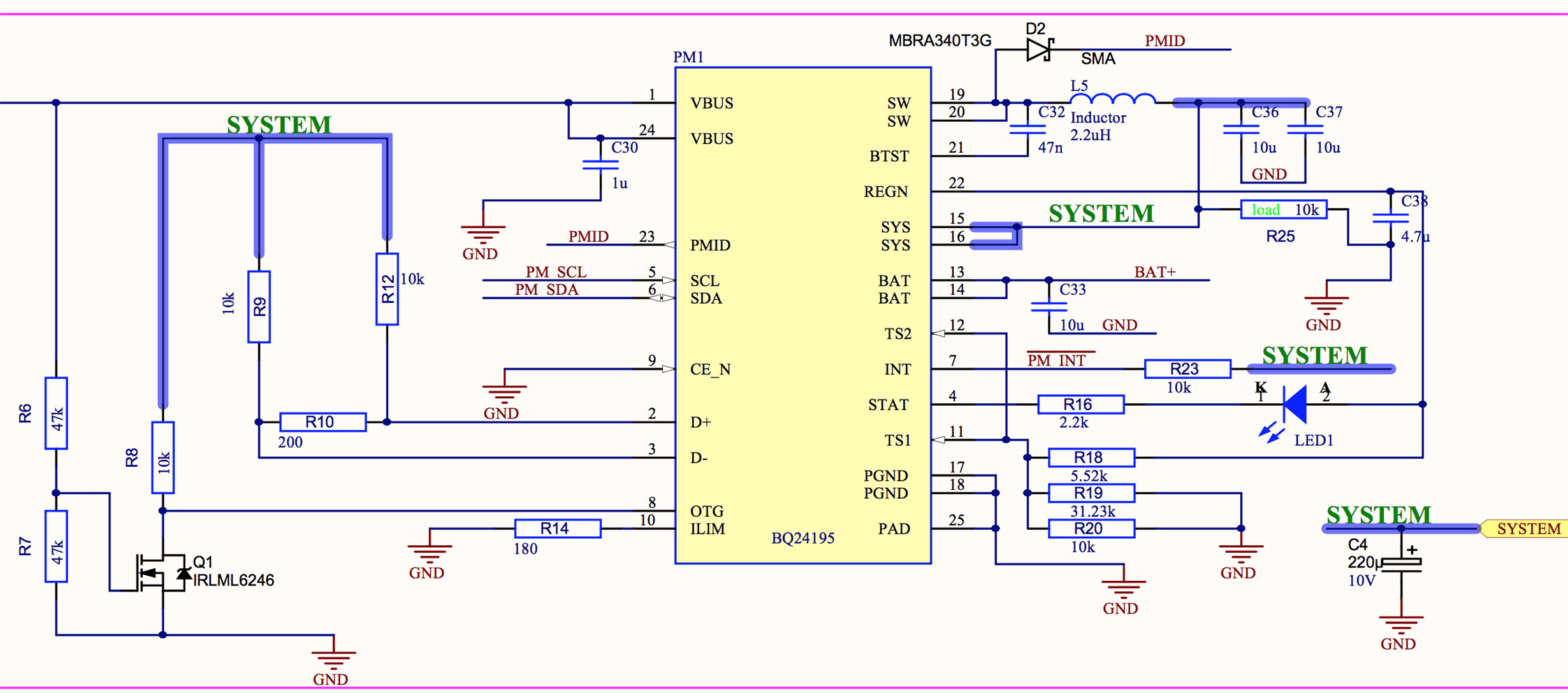
We've made a board with power management block based on BQ24195. Here is the circuit:

On PMID we have 60uF ceramic + 220 uF electrolyte. VBUS gets powered from 5V source, we also have a battery connected.

The purpose is to charge the battery permanently and get 5V from the battery when VBUS is off. Current consumptions are <500mA from PMID and <3A from SYS.

We have our host computer's power connected to PMID pin of BQ, but it gets off when VBUS gets off, and as we found out, this BQ cannot automatically switch to boost mode when VBUS turns off.

So, here is the questions:

1. Either boost or battery charging mode can be applied at the same time. Is that correct?

2. Is it wrong that we tied CE pin to ground and do not drive it from the host?

3. Can we somehow solve the problem with this or any other pin-compatible BQ?

4. It seems that BQ24295 is pin-compatible and has OTG and charge both enabled by default. But I'm a bit confused with that note: "3. Boost mode operation is enabled (OTG pin HIGH and REG01[5:4]=10)" which means that I have to turn off charging to enable boost, right?

5. Speaking about D+/D- detection. If we're not using them, do we have just to short it to make the highest input current limit? (We have pullups and 200 ohms there).

Thank you.

  • Hello Anatoly,

    1. The device can only operate on 1 mode at a time, either charging(buck mode) or OTG(boost mode for PMID). There's only one DC/DC converter in the device; when we go into OTG, we operate the buck converter in reverse.
    2.You can tie /CE to ground if you don't need to control it with the host. You can always disable/enable charger as well over I2C using the host using REG01[5:4].
    3.One thing to notice is that when you disconnect your input to allow OTG pin to go high, there will be a transition delay of ~220ms from when the device transitions from buck mode to boost mode, this is to ensure proper and safe transition. During this transition, the PMID voltage will go from ~VBAT at PMID to the OTG output once OTG starts. Majority of our devices that support OTG have this delay, meaning if your application requires an uninterrupted 5V source at PMID, you would need an additional power stage that can provide this rail. In this case, perhaps a buck-boost stage at SYS is more appropriate.
    4.Correct, similar to my answer to question #1, our chargers can only operate in buck or boost one mode at a time.
    5.Yes, if not using D+/D- you can short the pins using 200Ohms to set it to DCP by default. You can always overwrite the input current limit over I2C after POR.

    One thing, in order for OTG to start, there are several conditions that need to be met:
    1. BAT above BATLOWV threshold (VBATLOWV set by REG04[1])
    2. VBUS less than BAT+VSLEEP (in sleep mode)
    3. Boost mode operation is enabled (OTG pin HIGH and REG01[5:4] = 10)
    4. After 220-ms delay from boost mode enable

    The gating action to enable OTG after the input is removed will be item#2. Your host needs to modify REG01[5:4] to configure the device to OTG, hence why the device won't transition to OTG automatically upon input removal.
  • Hello Fernando,

    Thank you for fast response.

    Speaking about alternatives - can we use some another BQ (like BQ25895) with Integrated Control to Switch Between Charge and Boost Mode? It does not require external host to switch between charge and boost, right?

    But BQ25895 is not fully pin compatible as I can see - there will be short-circuit on DSEL pin during input type detection phase. Could you please recommend some more suitable device (if it exists)?

    Thank you.
  • Hello Anatoly,

    Yes, OTG is enabled by default on the bq25895, meaning if the other conditions for OTG are met upon input removal, the device should go into OTG without host intervention. Having said that, there's still a transition delay from charging to OTG of ~30ms. Whether this delay is tolerable will depend on the application requirements.