This thread has been locked.

If you have a related question, please click the "Ask a related question" button in the top right corner. The newly created question will be automatically linked to this question.

UCC27211: Bootstrap supply questions

Part Number: UCC27211
Other Parts Discussed in Thread: CSD18535KCS, LM5101A

Dear sir,  

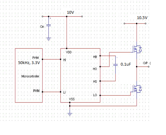
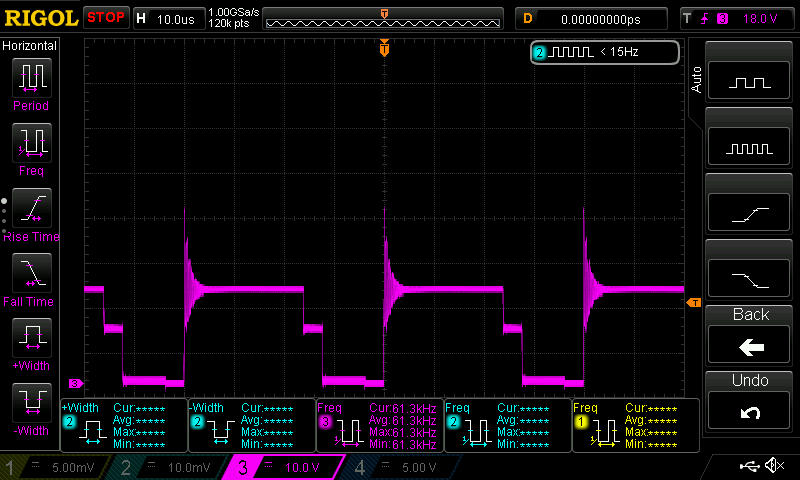
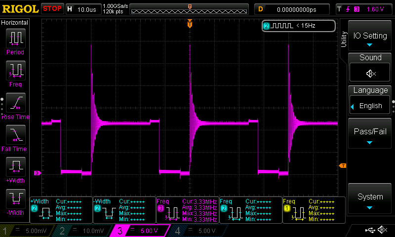
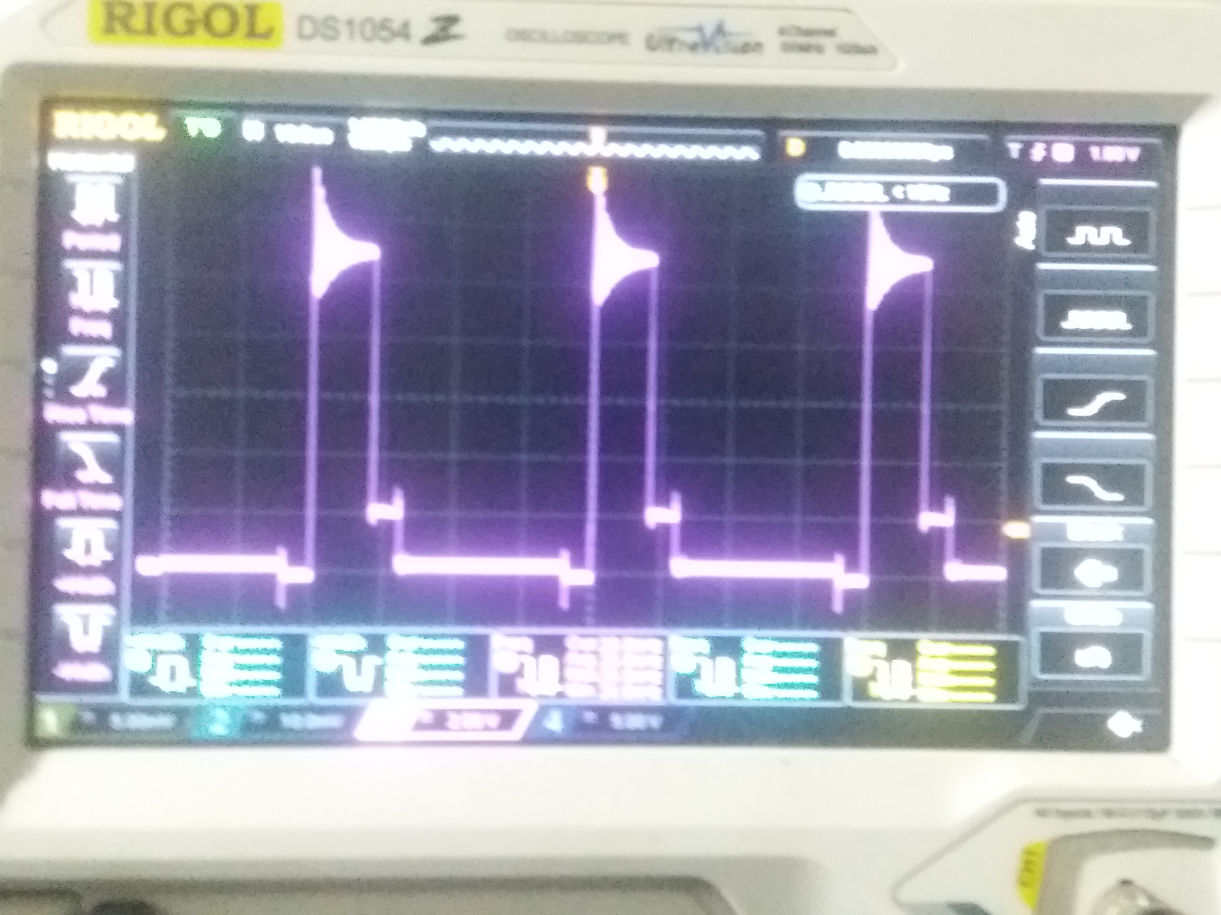
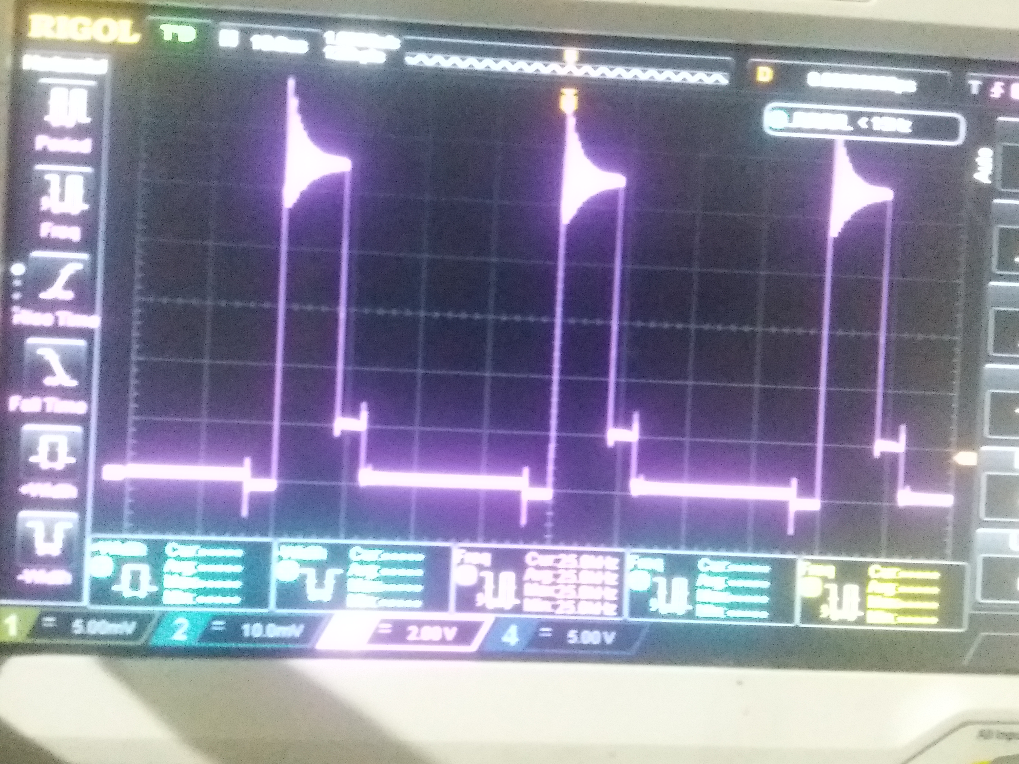
I have been using ucc27211 to drive High side mosfet. But I for not get the desired output. The output waveform was as shown in the diagram below. How can I reduce the ripple so as to get the desired ouput?

  • Hello Hitesh,
    Thank you for the interest in the UCC27211. To help with your question and concerns I need a little more information.
    Can you confirm the waveform that is on the scope plot, signal name, amplitude and time scale. It looks like it is the HS pin on the driver, or the HO pin to ground.
    If this is the HO to ground signal, can you provide a graph of the HO to ground and HS to ground, or preferred would be a graph of the HO-HS differential signal and HS to ground.
    The ringing is likely on the HS signal to ground.
    Can you provide a diagram or description of the circuit? Type of converter, input voltage, output voltage, and load current of the conditions of the plots.

    Regards,
    Richard Herring
  • I m using UCC27211 to drive high side mosfet for synchronous BUCK converter. 
    Input Voltage to the drain of High sode Mosfet is about 40 V maximum.
    And Input to the UCC27211 is 10V. 
    The waveform shown in figure is at no load condition. 
    I have used Bootstrapping capacitance of 
    0.1 uF and the input PWM Input is 3.3 V at 50 KHz.
    The output waveforms attached are at 10.5 V input to Drain of High side mosfet.
    Circuit Diagram.
    Fig1.HO and ground

    Fig2.HS and ground


    Fig3. LO and GND

     
  • Hello Hitesh,
    Thank you for the more detail waveforms of the UCC27211 application. Looking at the second plot of the HS to ground, you can see the ringing exists on the switch node. Since the 1st plot is HO to ground, the ringing on HS with show up on this trace. Since the high side MOSFET is driven by the HO-HS differential, it does not mean all this ringing exists on the MOSFET Vgs.
    The waveforms look as I would expect regarding the HO, HS and LO in a condition where current flowing in the MOSFETs during the off time is conducting thru the MOSFETs body diode.
    When HO-GND is high the high side MOSFET is on and current is flowing during the MOSFET on condition. When HO-GND goes to the mid point the HO-HS signal is low, but the HS is still high due to current flowing in the MOSFET body diode, you can see the HS bump up slightly during this time due to the body diode Vf.
    When HS-GND is close to GND the LO is high and the low side FET is on. When HS-GND goes slighty negative the LO is off and the current flowing is conducting thru the low side FET body diode.
    When you have a condition where the low side FET body diode is conducting and you turn on the high side FET, you have to force the low side body diode to turn off which generates high current in the parasitic layout inductance and generates this high ringing. This is common in a sync-buck type application.
    To reduce the ringing you can try several things. 1) Look for a MOSFET with a faster body diode trr rating to turn off the body diode faster.
    2) Improve the layout with very short trace connections from the high side MOSFET drain to the Cin and low side MOSFET source to Cin. Adding a high frequency ceramic bypass capacitor close to the FETs can help a lot.
    3) You can slow down the turn on of the high side MOSFET by adding gate resistance, this will reduce the dV/dt when the switch node rises.

    Please confirm if this helps by selecting the green button on the thread.

    Regards
    Richard Herring
  • I m using CSD18535KCS MOSFET.Can u guide me what value of capacitor should I use.
  • Hello Hitesh,
    The LM5101A datasheet has good guidance on bootstrap capacitor sizing in Section 9.2.2.
    First determine Qtotal based on MOSFET and driver quiescent current and switching frequency.
    Q total = Qgmax + Ihbs(Dmax/Fsw = 81nC + 1uA(Dmax/50kHz) = 81.03nC. So the gate charge dominates compared to quiescent current.
    Cboot=Qtotal/deltaVhb. Where delta Vhb is ripple on HB cap.
    Worst case the HB ripple voltage should be VHB peak minus the worst case Vhb falling UVLO.
    This will be 10V VDD - boot diode drop, or 9.3V. VHB falling is ~7V worst case. So delta Vhb is 2.3V maximum.
    Cbbot=81nc/2.3V=35nC. We recommend considerable margin over this minimum value to account for capacitor tolerance with temp and voltage and possible skipped cycles on the Cboot recharge. So the 0.1uF shown is a reasonable value for the bootstrap capacitor.
    For CVDD, we recommend a 10x ratio to Cboot or 1uF for a 0.1uf bootstrap capacitance.

    Please confirm if this answers your questions with the green button on the thread.

    Regards
    Richard Herring
  • Dear sir, I'm not yet able  to resolvee my problem,

    Is there any problem in My designing, because My Cboot is also correct(.1uF)and I'm using CSD18535KCS MOSFET.

    PFA of my PCB board.

    Let me know what changes can I make.

  • Hello Hitesh,

    Thank you for providing the layout. If I can get a better understanding of what you are looking to improve on the waveform, we can try changes to improve the output signal. Is it the high frequency ringing you are looking to reduce? Or do you have a question why there is a step on the HS to ground waveform?

    I do have some comments on the driver layout that you provided. There are some things in the layout that can lead to gate driver ringing which can affect the operation of the power train.

    The trace routing from C4 (VDD cap) to pin 7 (VSS) is very long. This long trace will result in significant parasitic inductance in the gate drive current loop which can result in ringing on the Vgs. Can you try moving C4 close to the VDD and VSS pins to see if that helps.

    Also the routing traces from the C5/C6 HB cap to pins 2 and 4 are very long, this can also create the same issue with high parasitic inductance possibly causing high ringing in the Vgs waveform. Try locating C5/C6, or a single cap value equivalent close to Pins 2 and 4 of the IC.

    Can you tell me the purpose of the inductor shown in the layout? Is the switch node of the FET's driving the inductor as the load?

    Try the two suggestions on the driver layout, and confirm what is the desired output waveform you want to achieve. Or what are you wanting to improve.

    Regards,

    Richard Herring