This thread has been locked.

If you have a related question, please click the "Ask a related question" button in the top right corner. The newly created question will be automatically linked to this question.

LM26420-Q1: Load Regulation Issue

Part Number: LM26420-Q1
Other Parts Discussed in Thread: LP5912-Q1, LM26420

Hi,

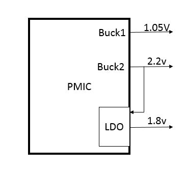
We are using TI PMIC LM26420-Q1 and LDO LP5912-Q1 in our automotive design solution.

The schematics for the supply are as shown

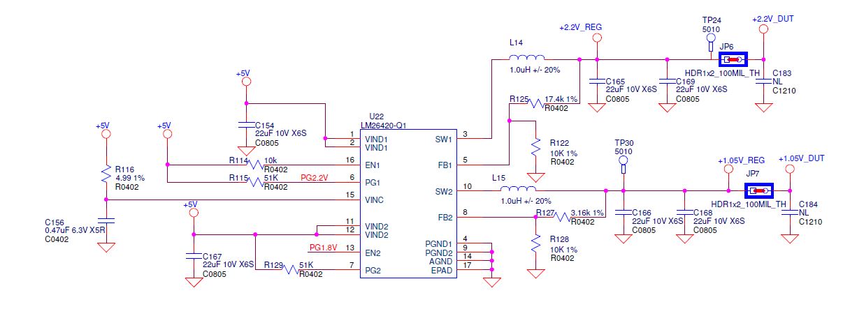
The 2.2V output from the BUCK is fed to a switching load and also goes as input to the LDO. The 1.8V output from LDO goes to analog circuitry. The switching load and analog circuitry are on the same chip and we have decoupling capacitors of value 10uF, 2pF for 2.2V rail and 0.1uF for 1.8V rail near the chip.

We are observing spikes due to switching at 2.2V output and 1.8V output at room temperature. At 105C, the amplitude of spike is more and is causing performance degradations.

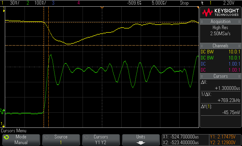
The output observed during transmission at 25C:
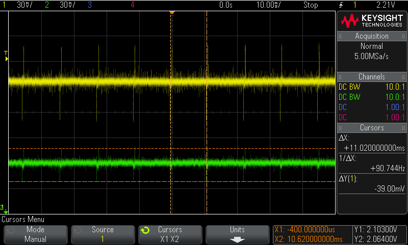
and at 105C:

Yellow corresponds to 2.2V buck output, green to 1.8V LDO output.

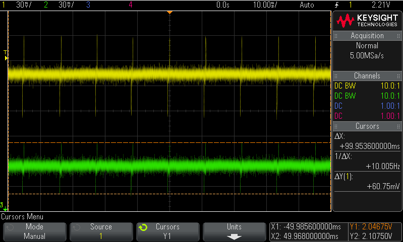
The performance is improved at 105C by using a 47uF Capacitor at 1.8V LDO output:

Even at 25C, with 47uF capacitor, the spikes are reduced as:

Currently Cap value >47uF needs to be used at output of 1.8V to improve performance. The capacitor value seems too large and will increase BOM cost. Also this seems like a quick fix and we are not sure of the root cause of the issue.

Do you have any suggestions to root cause the issue and improve performance?

In our previous design we used a different make PMIC, on which such issues were not observed. In current design we replaced the PMIC with TI solution keeping everything else the same, that is, the load and the decoupling capacitors near the load.

Previous PMIC was a dual buck + LDO single chip solution.

Output from the previous PMIC is coming as:

What changes do you suggest to get a clean output from the TI PMIC and LDO?

  • Sreejith,

    Can you show a zoomed in waveform? let's start with the 2.2 V output. I need to see both the output voltage and the SW1 voltage. Try 500 nsec/div. we need to determine if you are seeing switching noise or some other artifact.
  • Hi John,

    Here is the zoomed in waveform:

    Yellow trace is the output across C165, after L14. Green trace is at SW1.

    What we observe should be due to load switching. It is only present while the PA is ON, as shown in below zoomed out capture:

    Below is the waveform while PA is OFF:

    Regards,

    Sreejith

  • Sreejith,

    OK, we have established that switching noise is not your issue.  You are getting larger ripple due to your load condition.  Can you tel me about "PA"?  From your waveform it looks like it is "on" for about 180 usec, then switches "off" and then back "on" rapidly.

  • Hi John,

    It's a duty cycle based RF Power Amplifier. The spikes are aligned with dutycycle of operation. These spikes are leaking into the 1.8V LDO output, which is causing performance degradations.

    Regards,
    Sreejith
  • Sreejth,

    You will need to increase the output capacitance.  For a load step, when the current is changed suddenly all the additional current must be supplied by the output capacitance until the loop can adjust.  Also lower value output inductor and wider loop BW can help, but primarily you will need to increase the output capacitance.  Do you know the load step amplitude and slew rate? 

  • Hi John,

    We have tried increasing capacitance values, and also with reduced inductor values at 2.2V output. But there is no significant improvement in the spikes.

    Our main concern are:

    • Spike at 2.2V buck output at 25C itself, which gets coupled to 1.8V LDO
    • Spike at 1.8V LDO  (LP5912-Q1) output at 105C (60 mVpp) is higher than at 25C (40mVpp). This increase in spike amplitude is causing peformance degradation at 105C.

    Could you suggest any other solution for reducing the spike ?

    Regards,

    Sreejith

  • Sreejith,

    How much increased capacitance did you try?  Can you tell me about the load step profile amplitude and slew rate?  From that I can estimate how much additional capacitance is required.

  • Hi John,

    These are the voltage and current waveforms captured with the original values of L and C ie 1uH and 2 x 22uF:

    Yellow trace corresponds to voltage and green to current.

    The current is rising at ~300mA in 1.3us.

    Regards,

    Sreejith

  • Hi John,

    Did you get a chance to check it out

    Regards,
    Sreejith
  • Sreejith,

    You might want to consider a drastic increase.  Can you go as high as 2 x 100 uF + 1 x 22 uF?

    Let me know if that will work for you.

  • Hello John,

    Thanks for the support!

    I am Chaitanya Rathi working with Sreejith on this project.

    Adding 2x100uF caps is not a feasible option for our design. Do you have any other solution for reducing spikes on 2.2V?

    As mentioned earlier by Sreejith, we were using non-automotive PMIC in our earlier revision, where we did not see such spikes. We had only 1uH and 10uF combination at 2.2V buck output in that PMIC design.

    Is LM26420-Q1 PMIC not able to handle such switching in load?

    Thanks,
    Chaitanya
  • Chaitanya,
    What you are observing is specifically "load step transient response". The output current of the converter cannot change instantaneously. When the load current suddenly increases, the initial extra current must be sourced form the energy stored in the output capacitors. This will cause the output voltage to reduce and the closed loop control loop will allow for the converter output current to increase to the new load level as well as recharge the output capacitors to the desired regulated voltage. When the load current is suddenly decreased the inverse happens, the excess load current flows into the output capacitors and causes the output voltage to rise up above the desired regulation point. The internal control loop will respond ad reduce the output current and the output voltage returns to the desired regulation point.

    The factors involving the amplitude and recovery time for transients are primarily the output capacitance and ESR. You are already using low ESR ceramic types.

    Next is the control loop BW. For LM26420 it is essentially fixed internally.

    The speed at which the current can ramp up or down is determined by the inductor value. You may get some performance improvement by decreasing the inductor value. It does not has as large an effect as increasing the output capacitor.

    Also, you state your previous PMIC only had 10 uF output capacitance.  I would be surprised if it performed as well as your current circuit with 2 x 22 uF on the out put and the same inductor.  Is it possible your load step has a faster slew rate or higher amplitude now?