A related question is a question created from another question. When the related question is created, it will be automatically linked to the original question.
If you have a related question, please click the "Ask a related question" button in the top right corner. The newly created question will be automatically linked to this question.
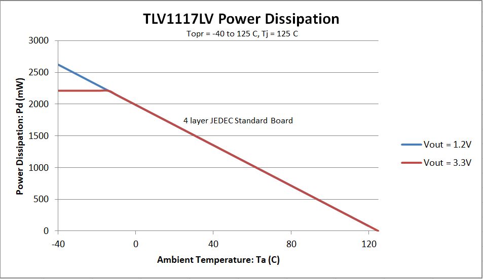
TLV1117LV33EVM-714: POWER DISSIPATION vs. AMBIENT TEMPERATURE of TLV1117LV
Power Dissipation vs. Ambient Temperature can be constructed based on values given in the datasheet. An LDO's junction temperature is a function of both the ambient temperature and power dissipation.
Tj = Ta + Rja * Pd
The maximum recommended junction temperature for the TLV1117LV is 125C. Rearranging the above equation using Rja = 62.9 C/W gives the following equation for a line where Ta is the independent variable and Pd is the dependent variable. This can be plotted using excel or other graphing software:
Pd = (125 - Ta)/62.9
In some cases, like in the datasheet you linked, the device has a maximum allowable power dissipation regardless of ambient temperature. This is calculated as:
Pd,max = Io,max * (Vin,max - Vo,min)
TLV1117LV devices are fixed output ranging from 1.2V to 3.3V. They all have a maximum 5.5V input and 1A load current. Pd,max then ranges from 2.2W to 4.3W. As you can see from the graph, the curve will only flatten off at lower temperatures in the case of higher output voltage versions.
Keep in mind that the actual thermal resistance, Rja, depends heavily on board layout. The value given in the datasheet is determined based on the 4 layer High-K board described in JEDEC's JESD51 industry standard.