Because of the holidays, TI E2E™ design support forum responses will be delayed from Dec. 25 through Jan. 2. Thank you for your patience.

This thread has been locked.

If you have a related question, please click the "Ask a related question" button in the top right corner. The newly created question will be automatically linked to this question.

UCC27714: High side mosfet abnormal turn off when double pulse test

Part Number: UCC27714

Hi Guys

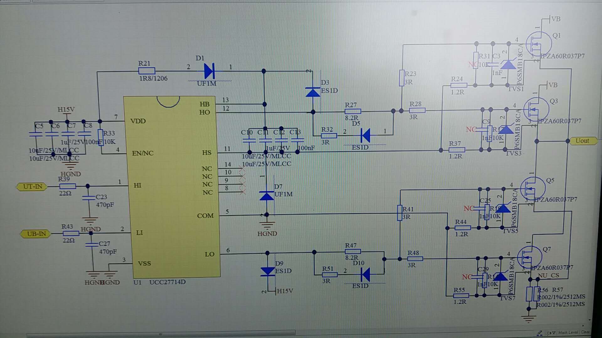
Our customer are using our UCC27714 to drive a half bridge mosfet in three-phase inverter application.  high side and low side mosfet contain two mosfets in parallel. you can see the Schematic in which I just show U phase. there are V phase and W phase that are the same as U phase.

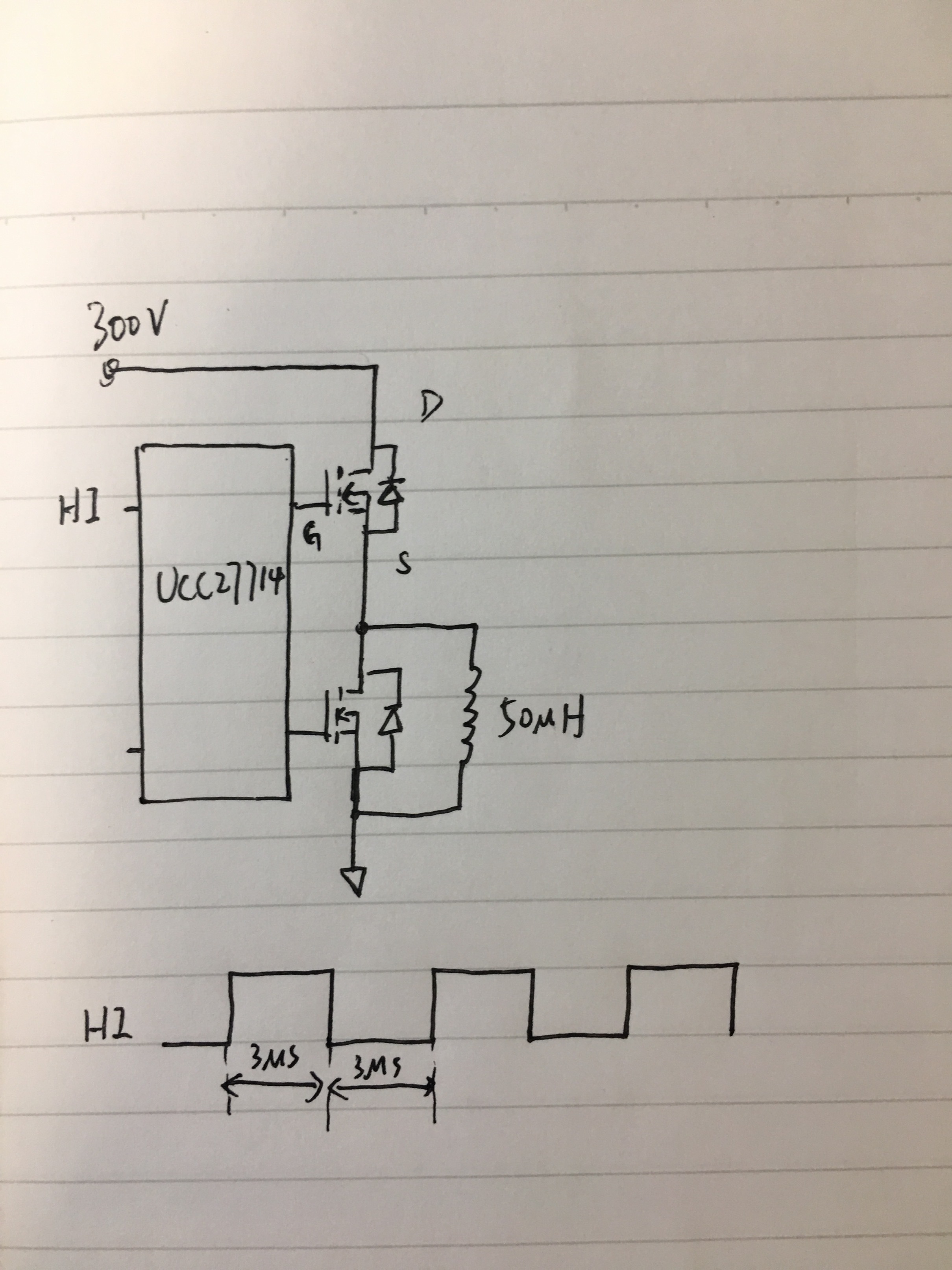
When customer do the double pulse test. Test circuit is below: which we call it high side mos test.

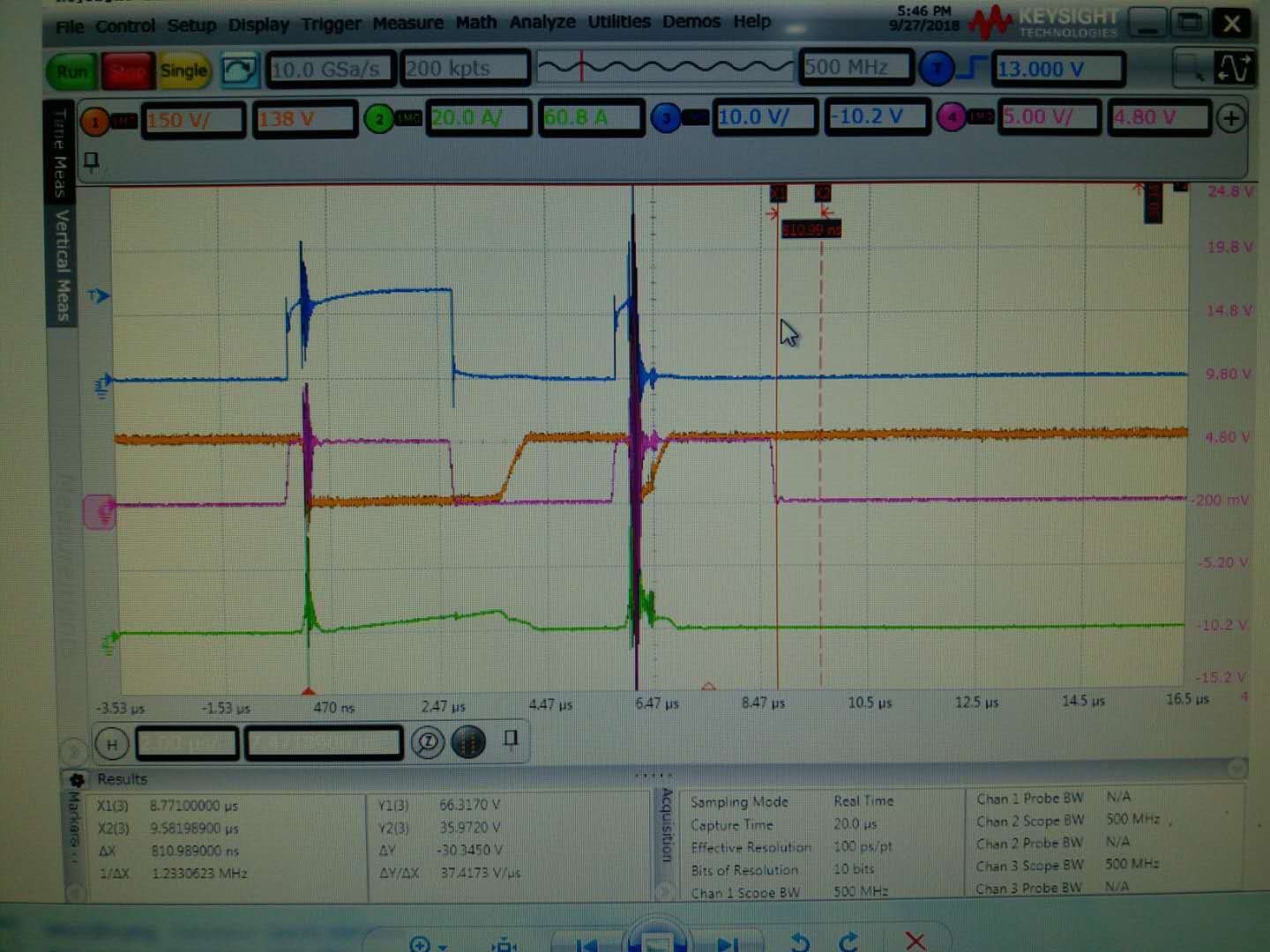
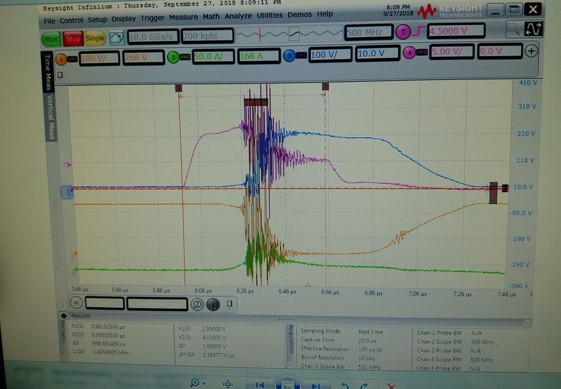
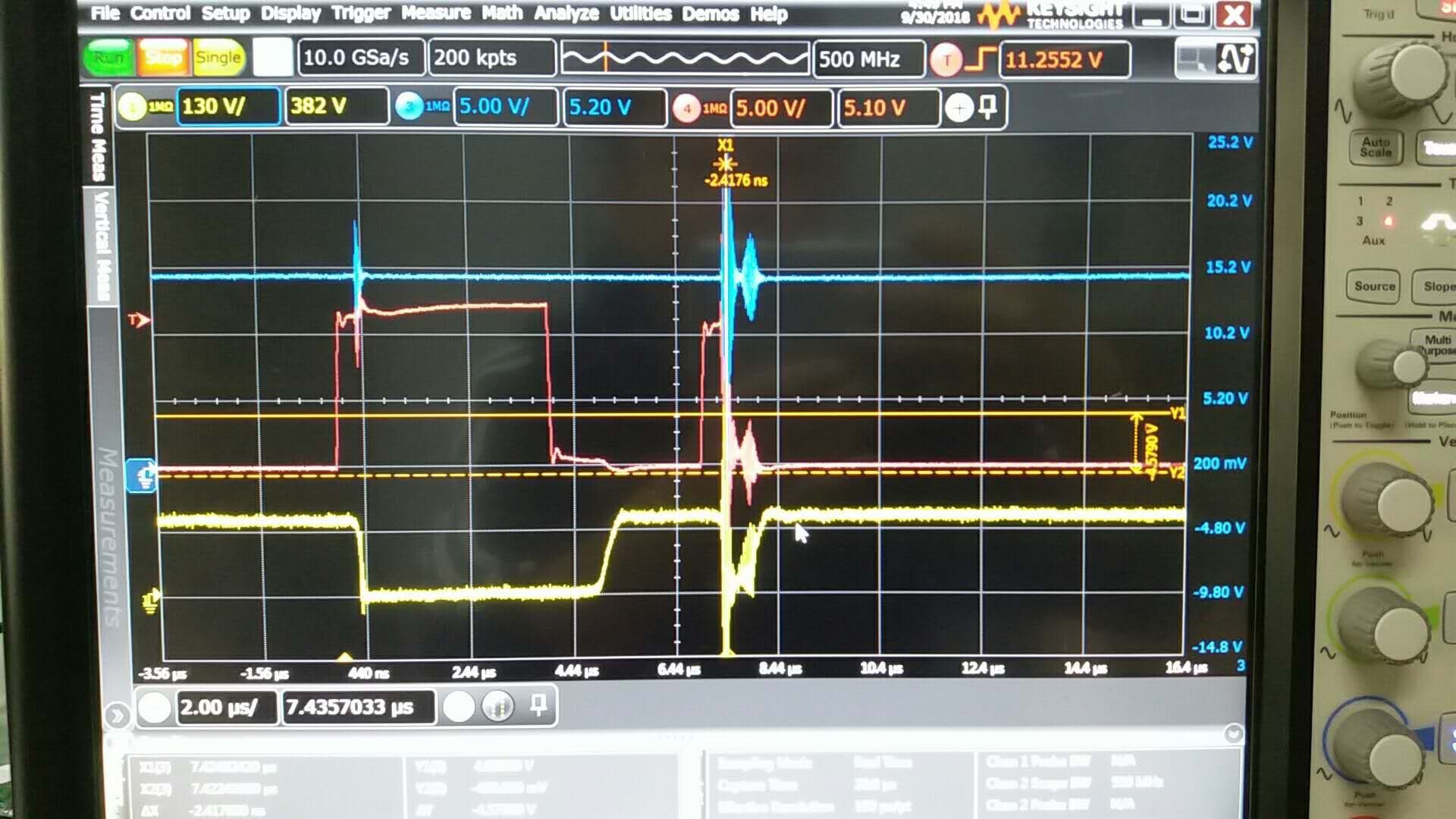
At this test, we found an issue:  Sometimes, the first pulse is OK, but at the second pulse ON, the high side driver will turn off abnormally. you can see below:

CH1:Vds;    CH2: Ids;     CH3: HO Pin;     CH4: HI Pin;

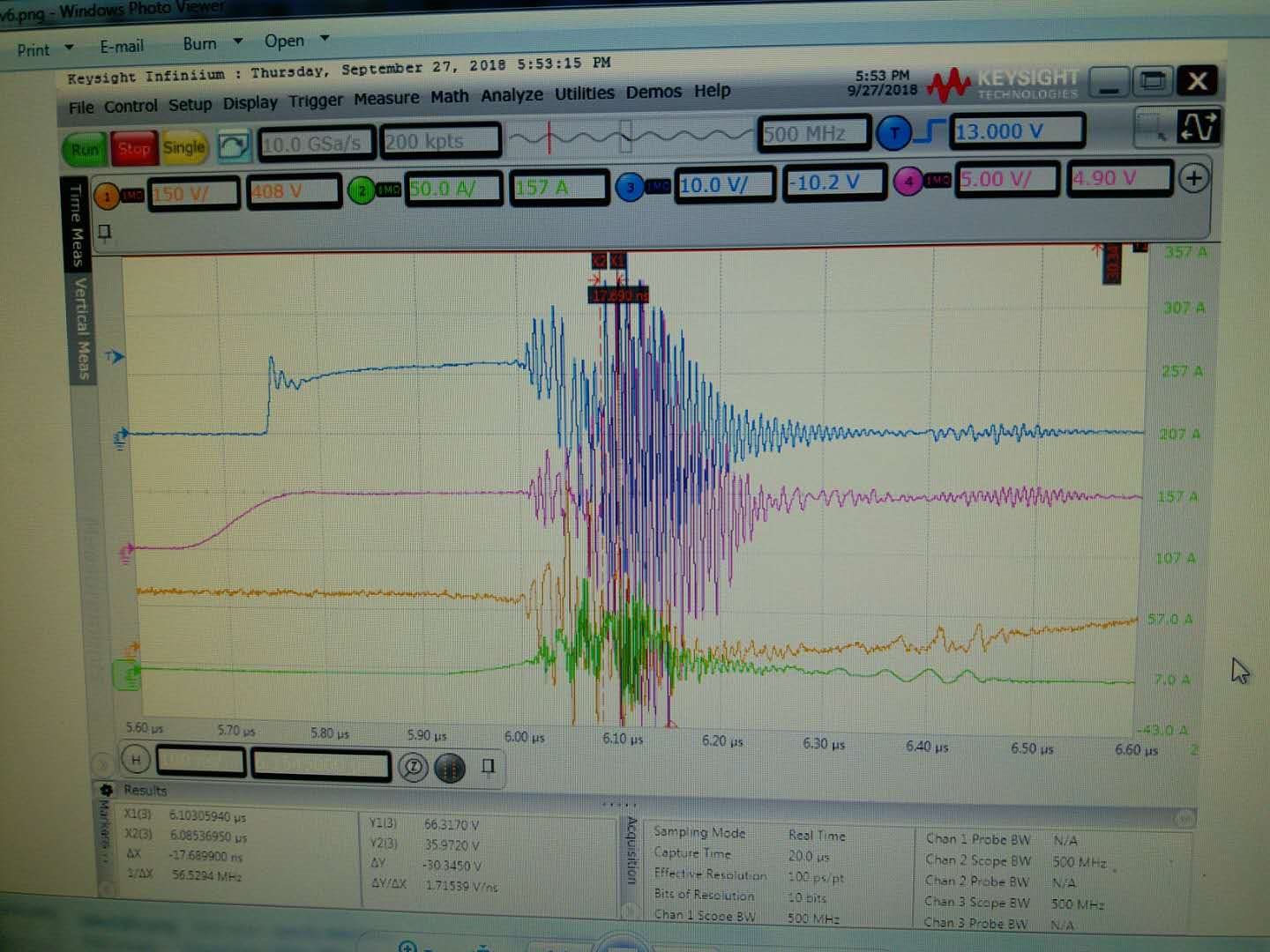
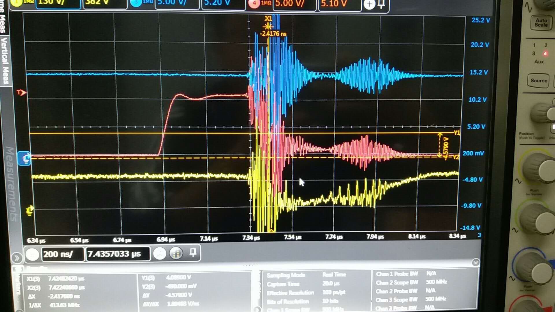
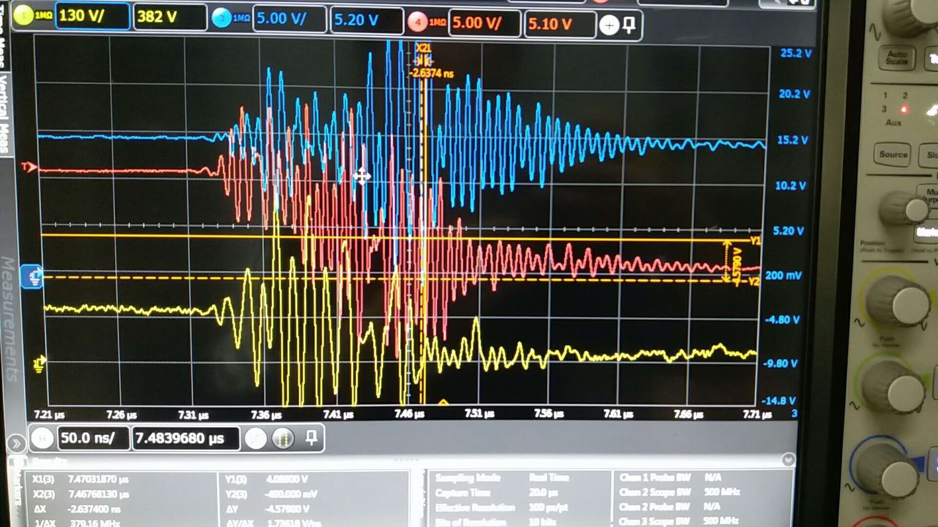
Zoom In at the event point:

I also asked customer to test the HB pin at the time of event. There are too many pictures. I will post the other pictures at the reply section.

Thanks

-Vincent

  • I also asked customer to test the HB pin at the time of event:

    because I find some explanation about the output logic problem on the Page25 in the datasheet.

    In the whole double pulse test, the low side mos test is all normal.

    In addition, I asked customer change a lower boot cap 1uF to test again. The high side mos test issue is still occur.  So my question:

    Why the second pulse HO will drop when the mosfet is turning on? How to solve this problem?

    I checked the PCB trace on the board, I found the high side drive trace is very long. I am not sure if it is related to its PCB trace. But if it is, do you have any suggestion for this?

    Could you please help me review this issue? Any feedback are appreciated.

    Thanks 

    -Vincent

  • HB pin waveform:

    CH1:Vds; CH2: Ids; CH3: HB-Vss ; CH4: HO Pin;

    The pulse:

    high: 3us; low: 3us;

  • Hello Vincent,
    Thank you for supporting the UCC27714 with our customer.
    In looking at the waveforms, it looks like when the high side switch turns on there is a lot of high frequency ringing. You can see on the scope plot, even the 1st pulse when the current starts flowing there is a burst of high frequency ringing on HO then the high side drive keeps rising. On the second pulse the HO has an early termination of the pulse during the ringing.
    The very long trace on the PCB layout is a concern, as this will result in high parasitic inductance in the gate drive loop, this parasitic inductance along with the MOSFET capacitance forms a resonant circuit which is excited during the switching transitions.
    If the UCC27714 outputs ring below ground there can be concerns with maintaining the correct output state. I see that there is a diode from the gate to source of the MOSFET which looks located close to the MOSFET, and a diode from HO to HB this part should be located as close to the UCC27714 HO and HB pins as possible. To limit the negative voltage on HO to HB add schottky diodes from HO to HS as close to the IC pins as possible.
    To reduce the ringing during the MOSFET turn on there can be a few things to try. Increase the R27, turn on gate resistance which will serve to reduce the dV/dt of the Vgs and Vds of the Mosfet. Also this higher resistance will lower the Q of the gate driver loop from driver to Mosfet gate and source.
    I see a placeholder for a capacitor on the MOSFET gate to source. Installing capacitance on the gate to source can also help in two ways, the additional capacitance will result in less Vgs deviation when the Mosfet switches and the parasitic drain to gate miller charge is transferred to the gate terminal. The miller charge transfer is likely what starts the ringing on the gate drive waveforms. Also the capacitance will serve to also slow the Vgs dV/dt which will reduce the Vds dV/dt therefore reducing the peak current transferred into the gate from the miller capacitance.

    Let us know if any of these suggestions resolve the issue.
    Regards
    Richard Herring
  • Hi Richard

    Thanks for your support about this issue. Please see below my question:

    (1)"If the UCC27714 outputs ring below ground there can be concerns with maintaining the correct output state. I see that there is a diode from the gate to source of the MOSFET which looks located close to the MOSFET, and a diode from HO to HB this part should be located as close to the UCC27714 HO and HB pins as possible. To limit the negative voltage on HO to HB add schottky diodes from HO to HS as close to the IC pins as possible. "

    Vincent: I will have a try to put the diode close to the IC by jumping wires. is it OK?

    (2)"To reduce the ringing during the MOSFET turn on there can be a few things to try. Increase the R27, turn on gate resistance which will serve to reduce the dV/dt of the Vgs and Vds of the Mosfet. Also this higher resistance will lower the Q of the gate driver loop from driver to Mosfet gate and source."

    Vincent: I will try to different values on R27. But due to the drive current limit: (15V-0.6V)/10ohm=1.4A. I will try 10ohm  and 15ohm. Is it OK? Or what is the maximum value on R27?

    (3)"I see a placeholder for a capacitor on the MOSFET gate to source. Installing capacitance on the gate to source can also help in two ways, the additional capacitance will result in less Vgs deviation when the Mosfet switches and the parasitic drain to gate miller charge is transferred to the gate terminal. The miller charge transfer is likely what starts the ringing on the gate drive waveforms. Also the capacitance will serve to also slow the Vgs dV/dt which will reduce the Vds dV/dt therefore reducing the peak current transferred into the gate from the miller capacitance."

    Vincent: I will put the capacitor between the Gate and Source. But could you tell us how to choose the cap value? What is the specific way to calculate the value? I think it should be close to parasitic capacitance of mosfet. IPZA60R037P7 DATASHEET: Ciss=5243pF; Crss=1599; So Cgs=5243pF-1599pF=3.6nF... So I will have a try 1nF~10nF cap on it. Is it OK?

    Thanks

    -Vincent

  • One more point: what cause the low output of the UCC27714 ? what will the Too large Ring affect? UVLO or some others?
    Thanks
    -Vincent
  • Hi Richard

    I have tried all ways but the abnormal turn off still occurred.  I have put the diode close to the IC by jumping wires; R27=10ohm(15 ohm will be worse); Cgs=10nF; I also asked customer capture some waveforms:  

    CH1: Vds(YELLOW); CH3: VDD-VSS(BLUE); CH4: HO-HS

    Zoom in:

    We can see some rings will go down to below 4V for VDD-VSS. I doubt it because of VDD UVLO. Some times the pulse will be normal but the ring also reached to below 4V for VDD-VSS. So maybe it is not related to the VDD voltage.

    So I really want to know what cause the low output of the UCC27714. what will the Too large Ring affect? UVLO or some others? 

    Your feedback are appreciated.

    Thanks

    -Vincent

  • Hello Vincent,
    For the placement of the clamp diode from HO to HS, using jumper wires for the connection is likely not adequate as the wires will have parasitic inductance and will not effectively limit the potential negative voltage.
    For the cause of the abnormal pulse, if the HO voltage goes below HS this can cause current to flow in the IC internal circuits which can result in the HO going to the incorrect output state. Can you try physically relocating the diode and placing as close as possible to the IC pins?
    Something else I see , which may result in pertubations on the MOSFET Vgs is the R37 resistor from HS to the MOSFET switch node. Can you ask the customer to try placing a zero ohm jumper for R37?

    Regarding the specific questions: Using jumper wires for the connection of the HO to HS clamp diode will likely not be effective in clamping the voltage.
    For the maximum value of R27, this depends on the application specifically what is the dead time from LO and HO, make sure the MOSFETs can turn off in the dead time, and at the application switching frequency is the switching loss OK for the user. The 15 Ohms mentioned should not be a concern for the turn on gate resistance.
    For the recommended added capacitance on the gate. What this helps is when the MOSFET switches the miller charge conducts current into the gate during the VDS rising time which will reduce the voltage on the Vgs. The additional capacitance will help reduce the negative Vgs level during the Vds rising time. Since there is such long gate drive traces, you may need this to stabilize the Vgs at the MOSFET switch. The Qdg on this MOSFET is 37nC and Qgs is 27nC so the Qgd could remove all the charge on the Qgs in theory. With a 10nF capacitor and Cgs of 5.2nF, the Qgd could result in a 37nC/15nF or ~2.5V variation.

    On the scope plots showing large ringing on VDD. I would confirm if the scope probes are connected with short ground probe leads and the ground and scope tip are connected close to the VDD capacitor terminals. This is recommended test setup for all probes, the probes can indicate much higher ringing and peaks if the probe grounds and tips are not placed close to the IC pins.

    Regards,
    Richard Herring