Other Parts Discussed in Thread: TPS54540
Hi,
I'm working on a design based on the WEBENCH and TPS5450 converter. My issue is that I'm getting >2v p-p noise on output. I used the simulator but my real world results are troubling.
Specs
- 24V input
- 3.5A output
- 5V output
Components
- L: 12uH/23mR/ - SRR1260-120ML
- Cin: 20uF/20mR - GRM32ER71H106KA12L x 2
- Cout: 330uF/17mR - 6SVPC330M
- D: 5A/60V/100pF - SBR5E60P5-13
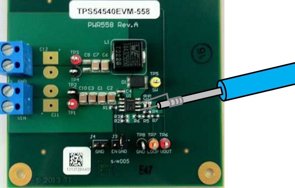
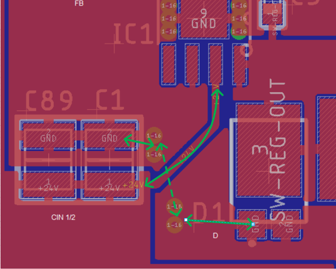
Circuit

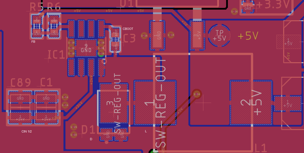
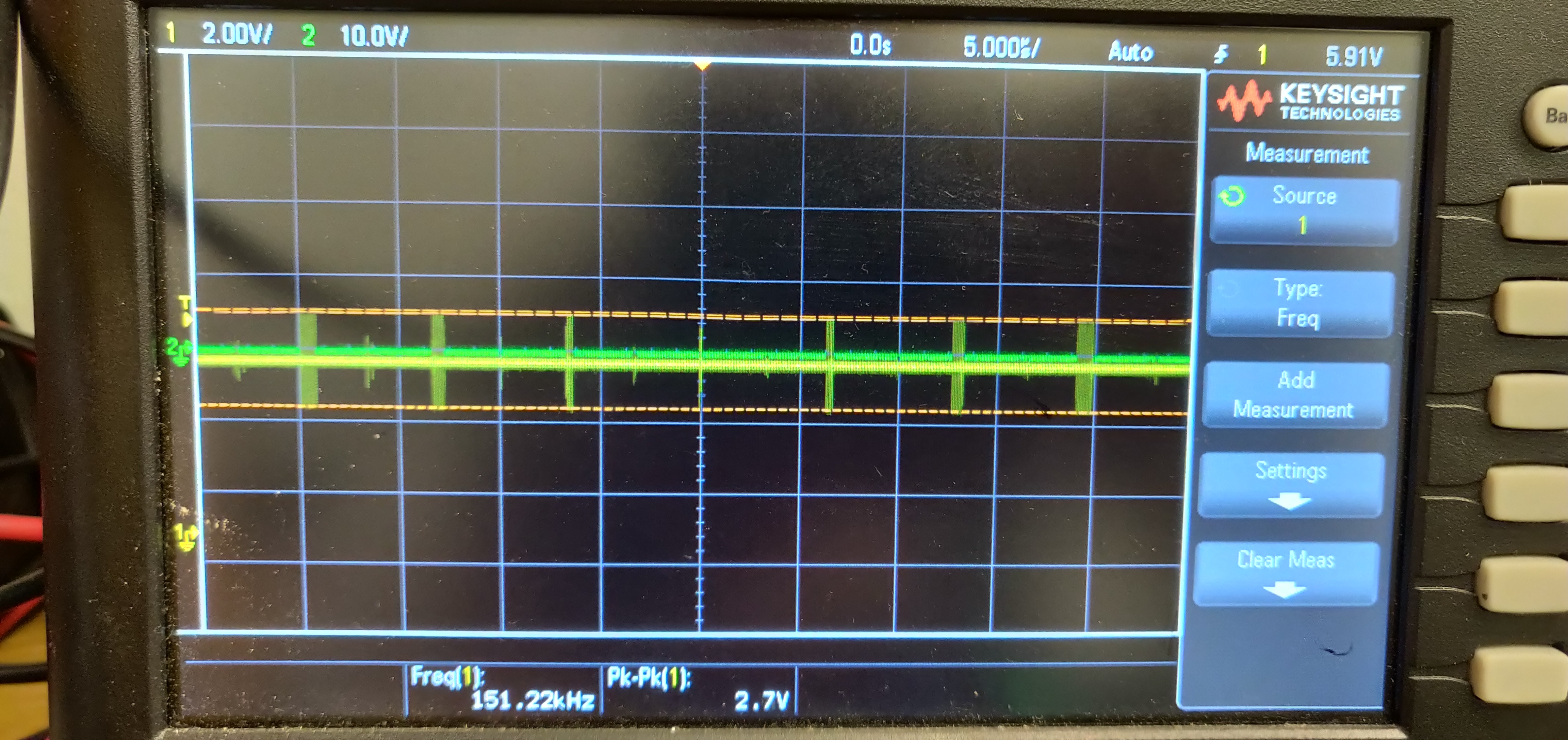
Problem
I'm getting 2V p-p noise on the 5V output. Also visible on inductor. Please see waveforms:

Solutions attempted
- Adding a 24R in series with Cboot
- Adding a snubber network (5R/110pF)
- Changing D to a B340AF-14
This helped but nothing like what it should. I wonder if it is the PCB but in all honesty have never experienced such an issue with a switching converter. Can it really be that sensitive?
Thanks for the support
Kind regards,
Charlie.