This thread has been locked.

If you have a related question, please click the "Ask a related question" button in the top right corner. The newly created question will be automatically linked to this question.

TPS1HA08-Q1: Automatic Switch On with Reverse Battery

Part Number: TPS1HA08-Q1

Dear, Sir.

My customer is applying Infineon's High-side IPD like BTS5016, so I am considering
how to replace it to TI's product.
An engineer complained that Infineon's products don't reflect the advantage standing on
system level usage such as Reverse battery. I thought TI's product would meet with his
expectation, the replacement could be realized.

I am so sorry ask you about this kind of fundamental matter, but hoping to get your
teachings to improve my poor understanding.

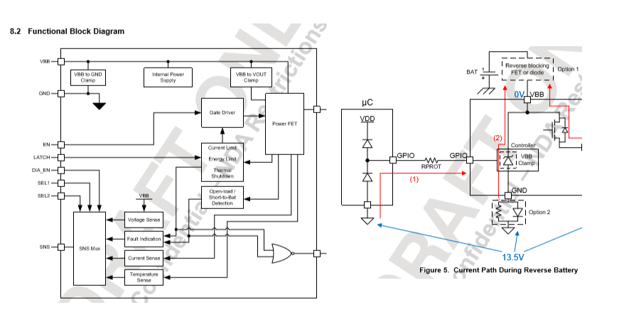
1. Integrated Power FET.
   Is it a NMOS FET?

2. Internal Power Supply.
   Is it a charge pump?

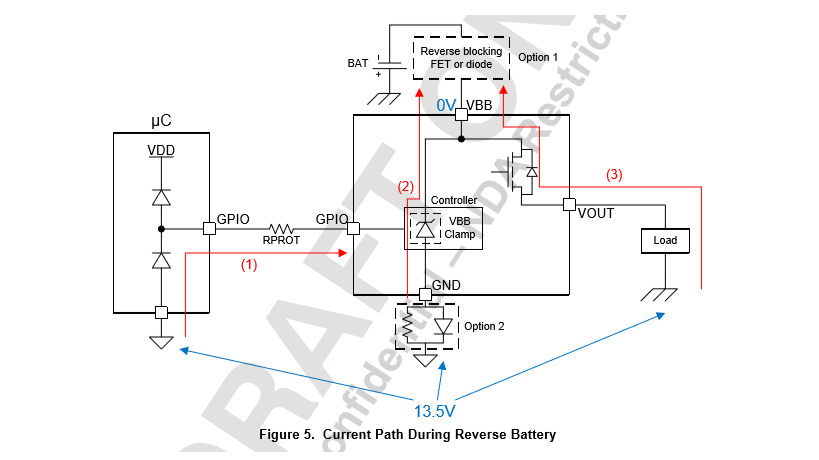
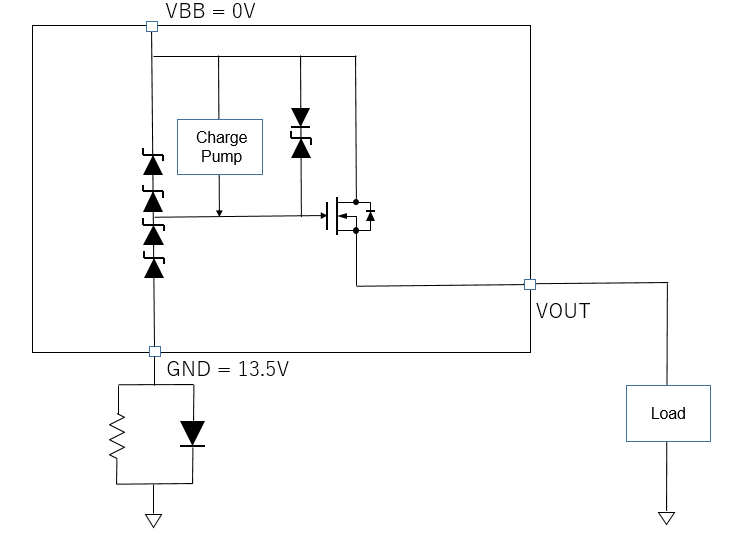
3. Automatic Switch On with Reverse Battery.
   Does it mean TPS1HA08-Q1 can be driven FET gate under reverse battery condition
   by biasing from GND side?
   How to realize that utilizing function blocks? I checked 8.2 Functional Block Diagram on
   DS, but not clarified yet.

Best Regards,

H. Sakai

  • Hello,

    1- Yes the integrated FET is NMOS

    2- Device has an internal charge pump to drive the FET

    3- Yes during reverse battery the FET is on. There is an inetrnal circuit biasing the gate and drives the FET fully on during reverse battery. The internal circuit is unavailable at this time.

    Regards  

  • Dear, Mahmoud-san.

    Thank you so much for all of your teachings.

    I would like to make sure the biasing path to the gate and FET fully on

    during reverse battery.

    I wonder the internal charge pump starts to work biasing FET's body diode as

    (3) path on Figure 5?

    Another scenario would be (2), but too much voltage drop will be occurred

    due to the external resistor & internal clamp diode.

    Sorry to ask this kind of matter, Hoping to get your teaching one more time.

    Best Regards,

    H. Sakai

  • Hello Sakai-san,

    The red color in the drawing shows the current paths during reverse battery. The charge pump is off but the FET gate is bias through the external resistor on input pin. This rises the gate voltage above the FET source voltage and FET is ON. Because VBB is at 0V and VOUT is at 0V as well, the FET gate voltage stays above the FET source voltage and FET stays ON.

    Regards

  • Dear, Mahmoud-san.

    Thank you so much for all of your valuable information & teachings. 

    I am guessing if VBB clamp would be configured with the stacking diodes as 

    below, Vgs(th) could be created. I wonder my assumption is correct? 

    Sorry to disturb your job gain & again. 

    Best Regards, 

    H. Sakai

  • Hello Sakai-san,
    I do not think the gate is biased through the VBB clamp as per your drawing. I do not have the internal circuit but we may ask for it from designer. We know the FET is on in reverse polarity. For what reason you need to know the internal circuit?
    Regards
  • Dear, Mahmoud-san.

    Thank you so much for your mentioning.

    They would like to know the purpose & reason of "Rgnd" value decision because
    it would be influenced to the device break-down.
    The exact circuitry is not needed.
    I am hoping to get your understanding & brief information about that.

    Best Regards,
    H. Sakai
  • There is an ESD cell from device GND and supply volateg VBB. In case of reverse battery, the ESD cell will be forward biased and the ground Resistor Rgnd should limit the current. The max forward current is 50mA and the min resitor is VBB/50mA.
    Regards
  • Hello,

    TI thinks the issue is resolved and the thread is closed. Please re-open it if you still have question.

    Regards