This thread has been locked.

If you have a related question, please click the "Ask a related question" button in the top right corner. The newly created question will be automatically linked to this question.

WEBENCH® Tools/BQ25895: PCB design with GND and PGND

Part Number: BQ25895

Tool/software: WEBENCH® Design Tools

My question is related with a complex design that includes in one PCB the bq25895 together with an LDO  and two uC. 

The idea is to use the bq25895 for charging a 1-cell LiPo battery. The Vsys output will be connected to an external 3V-fixed-LDO(TPS79730) to power one of the uC. The PMID output will be used to power another uC that works at 5V.  The system should work stand-alone (without VBUS connected) while the battery is charged, and afterwards, charge it with VBUS when it's needed. 

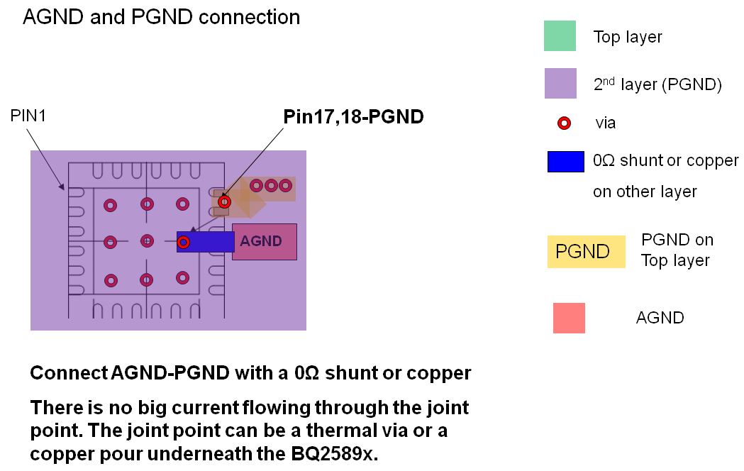
1- In the datasheet it's stated that PGND should be separed from AGND. In my design I have a PGND pour on top and bottom layers underneath the bq25895, the rest of the circuit (uC, sensors and LDO) has a GND pour. PGND and GND are connected only at one point using a VIA. Is this approach correct?. 

Thanks for your help. 

  • Hi,
    We are working on this query and will get back to you shortly.

    Thanks,
    S.Suganya
  • User1321,

    Moving to appropriate forum so an expert can answer your question.

    Thanks,
    Amod
  • Hi,

    Referring to 11.1 Layout guidelines on the d/s, please route analog ground separately from power ground. Connect analog ground and connect power ground separately. Connect analog ground and power ground together using power pad as the single ground connection point. Or using a 0Ω resistor to tie analog ground to power ground.

    The system example on the d/s shows the AGND and PGND connections.

    Below is example layout for AGND and PGND connection.

    Thanks,

    Ning.

    Please click "This Resolved my issue" button if this post answer your question.