This thread has been locked.

If you have a related question, please click the "Ask a related question" button in the top right corner. The newly created question will be automatically linked to this question.

TPS650830: 650830's LDO3V3 has fault output;

Part Number: TPS650830

Hi Experts,

While I was supporting one of our important customer, one important issue emerged. As the customer is using VR3 to generate a 3.3V output, which, has also been used as ENVR5 to enable VR5 when 3.3V ramps up. While I understood that the VRs were internally isolated and which pins related to VR3's output only included PGVR3, NVDCZ, VINVR3, ILIMVR3HS, ILIMVR3LS, FBVR3N, FBVR3P, VBSTVR3, DRVHVR3, SWVR3, DRVLVR3, PGNDVR3, ENVR3.

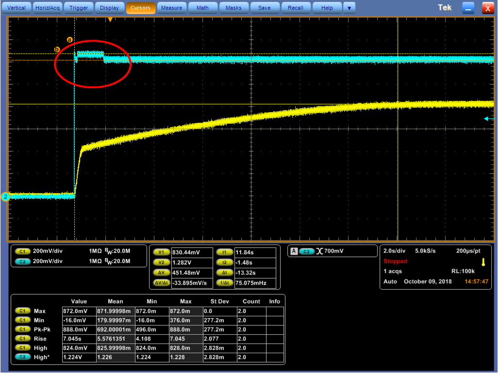
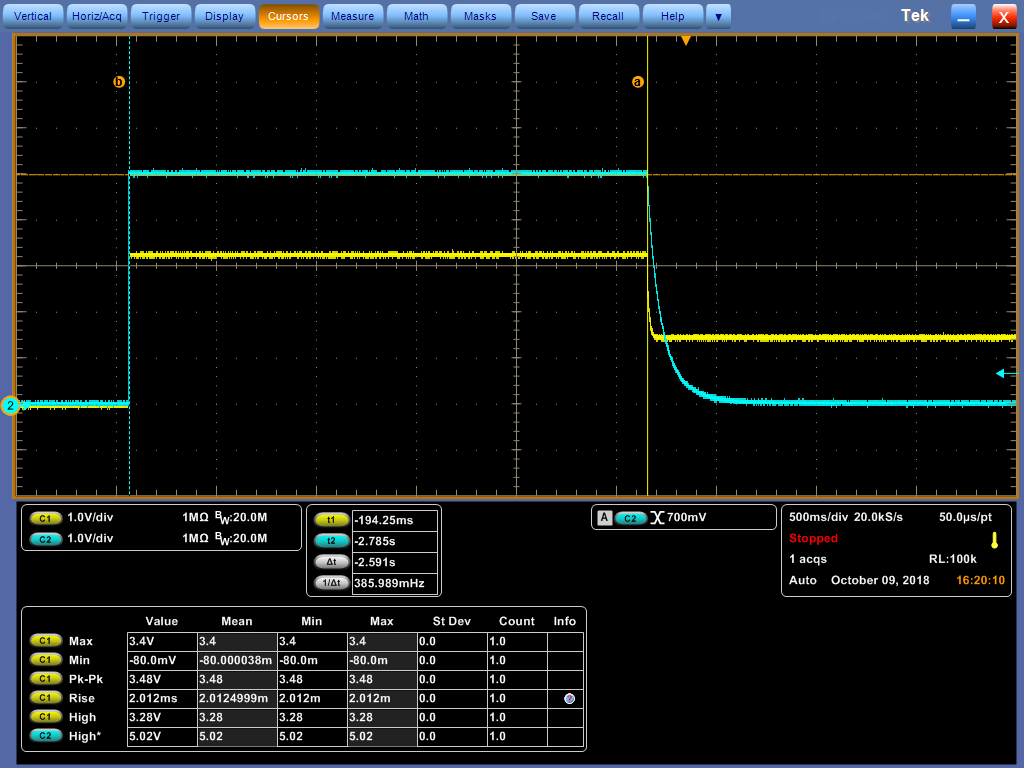
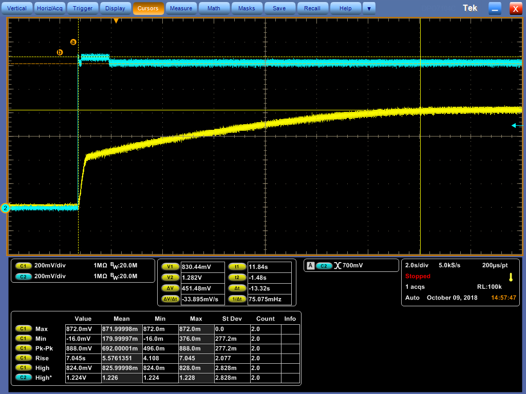
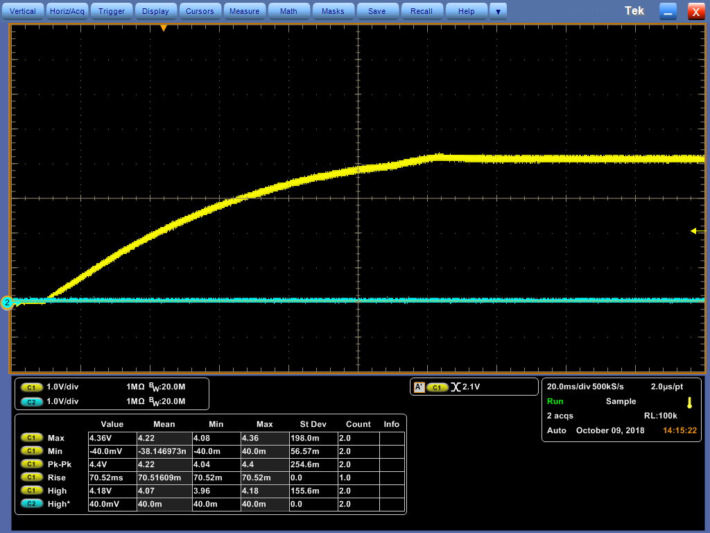
As the most critical pins that influence output are all above except PGVR3 and NVDCZ, the customer uses on-chip LDO3V to generate VR3's ENVR3 AND LDO5V to support VBSTVR3 and external 12V for VINVR3, VIN and VINLDO3, tending to make VR3 perform a 3.3V immediately after 12V powers on. However, 3.3V was not generated after power-on. While we were supporting them locally we found LDO3V had a really strange output shown as below and this issue happened randomly-> 16 pics in total, one of which LDO3V output is 0.84V and another output is 4.2V, note that all those 16 pics have totally same BOM and same layout. Those strange outputs have been suspected to be cause of making VR3 not output as 0.84V is too low to enable LDO5V and 4.2V is too large that might make internal logic disorder.

Note: Yellow line: LDO3V Output; Blue line VREF1V25 Output.

Note: Yellow Line: LDO3V Output; Blue Line: N/A


My question is,

1. What will cause LDO3V output unstably?

2. Merely from the waveforms, did those mean that two LDO3s do not work anymore?

Could you please comment this? Sorry by pushing you, but this is really emergent because they have been adjusting it for more than 30 days. Thank you for your great help!

-Wenhao

  • Hi Wenhao,

    One potential would be if the LDO3V is being overdrawn. It has a max current of 40 mA; is it being connected to anything that might be drawing more than 40 mA? If possible, can they try removing any pull-up resistors that they have connected to LDO3V one at a time to see if LDO3V will reach 3.3V after removing one such resistor?

    To avoid maximum current < 75 mA, total resistance must be less than 10 ohm so if any resistor are 10 ohm instead of 10k ohm for example that could create a problem or if any circuit powered by LDO3V requires high current just for start-up could create this issue.

    Alternatively, have they probed the VINLDO3 to confirm that voltage at the input capacitor for this pin is stable?

  • One other item to try is to externally pull LDO3V up to 3.3V and measure the current being drawn from the external supply to see if this is >75 mA.
  • Hi Kevin,

    Thank you very much for your reply. In customer's schematic, LDO3 is only connected with VDDIO_0, VDDIO_1, SHUTDOWNZ(100k pull-up), NVDCZ(100k pull-up), ENVR3(100k pull-up), VDDPG and ACOK. Merely from those pins it is pretty strange LDO3V could be overdrawn. Meanwhile, now the LDO3V is already outputting 4.2V, does it mean that the LDO inside is broken?

    Furthermore, in this following pic, Blue line is VREF1V25, why there is a strange transient change which has been red circled? Is it relevant to LDO5V Load switch? Thank you very much for your patient answering us!

    -Wenhao

  • Hi Wenhao,

    I was not able to verify the VREF behavior on an EVM today, but generally the voltage changing is the loading of the trim from the non-volatile memory. It is more accurate when the trim loads.

    As for the loading of LDO3 or why it would be 4.2 V, I did not see an obvious explanation for what could be happening on customer board. Was there any results from isolating the output or testing with external supply?
  • Hi Kevin,

    About results of testing with external supply, I will get back on you before next Tuesday. Furthermore the customer is asking us if we have EPLD's sequencing rules/documents conducted by TI and Intel together because they are utilizing both EPLD and 650830 to arrange power sequencing. Could you please tell me where i could find it? Thank you!

    Best Regards,

    -Wenhao

  • Hi Wenhao,

    I did not find such a document. The TPS650830 datasheet pg 45 shows the expected sequencing for the TPS650830 but the details on the EPLD are most likely available from Intel.
  • Hi Kevin,


    There is another thing I need your check about 650830. The customer found that output of VR3 and VR5 ramp up simultaneously and drop down after power on for approximately 2.6s. The detailed description and graph has been shown as below:

    • The Blue line is output of VR5(5VA_DS3), which ENVR5 is tied with output of VR3;

    • The Yellow line is output of VR3(3V3A_DSW), which ENVR3 is tied with LDO3V.

    From the graph it is clear that both output ramp up simultaneously. However, it is quite strange because originally it is output of VR3 which is supposed to ramp up first and then output of VR5 from right power sequencing.

    Furthermore, after both output power on for 2.6s, output of VR3 and VR5 drop down simultaneously to 1.5V and 0V, respectively. However, this phenomenon is still pretty abnormal as VR3 and VR5 should keep power on. I guess one possible cause is 650830 enters Emergency Shutdown State. I also suspect false power sequencing can lead to this “drop down” result.


    • Could you please point out that why those two output ramp up at the same time?

    • Could you please kindly clarify the reasons of two voltage simultaneously dropping down?


    Would it be OK for you to give an answer before next Monday? I will take it as a great appreciates if so. Thank you very much!

     Best Regards,

    -Wenhao

  • Hi Kevin,

    Inspiringly, after them re-weld the BGA pins, LDOs outputted normally. Thank you for your help. Furthermore they still have sequencing issues upon their demo. I will open another E2E thread.

    Thanks again!

    Regards,
    -Wenhao