This thread has been locked.

If you have a related question, please click the "Ask a related question" button in the top right corner. The newly created question will be automatically linked to this question.

TPS92518: VLEDx pin and shunt dimming

Part Number: TPS92518
Other Parts Discussed in Thread: TPS92515

I’m puzzled about the behavior of the VLEDx pin.

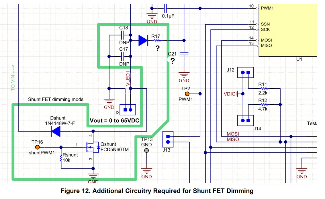
It is clear that in TPS92518 evaluation board with shunt dimming modifications, VLEDx will have a voltage closer to VLED * d, instead of VLED (where d is the shunt dimming duty cycle). It will have some ripple (low pass filter set at 159Hz), but since shunt dimming frequency will be >1kHz, it will be negligible.


I can see two issues with this:

  1. VLEDx ADC reading will not make sense, for two reasons:
    1. PWM pin is not switching, since I’m doing shunt dimming. So I won’t know if the ADC reading is made at off or on.
    2. Even if I read the ADC registers when I’m sure LEDs are on, the ADC reading will be VLED * d instead of VLED.
    3. The controller will not work in “constant μs*V” operation: even if the LED forward voltage will stay fixed, VLED pin will read a different voltage for each dimming duty cycle, thus the controller will set a different off-time for each duty cycle. This, as far as I understand, is unwanted. If I understand correctly this can be avoided by fixing VLEDx to a fixed voltage, “however current regulation degrades” as the datasheet says.


I think however that there is a solution for this. For a “similar” (but not quite the same) issue, TPS92515 datasheet (fig. 14) shows a diode between the driver output node and the pin that controls off-time. This diode, applied in our case in series with R17 in the evaluation board schematic, could make the circuit work as a “peak detector”, effectively making VLEDx pin voltage equal to LED forward voltage, approximately, independent of dimming. For this to work, C21 should be big enough to avoid being discharged too much by VLEDx pin input resistance.


What do you think of this issue? Has it been seen to compromise the performances?

What do you think of the proposed solution?

  • Hello Giaime,

    For shunt FET dimming at 1 KHz you do not want to use 10K and 0.1 uF filtering to Vledx. The diode clamp back to Vin, Dshunt, is better protection for long lines to the LEDs and clamping any ringing caused by shunt FET dimming. Reducing R17 to zero when using Dshunt allows the TPS92518 to read the actual LED stack voltage when Shunt FET dimming which will give accurate current regulation. It will also protect for open LED faults. C21 may need to be lowered or removed depending on how much Shunt FET switching loss you are okay with and EMI concerns.

    The off-time is generated externally on the TPS92515 so that diode behaves different than Dshunt, which is for protection.

    Best Regards,
  • Hello mr. Nederbragt,

    thanks for the reply.

    Yes a diode from output to power supply (Dshunt) is mandatory, I understand that. But that wasn't the diode I was talking about. See the picture below, I've sketched it based on the evaluation board schematic.

    In this configuration VLEDx pin always reads peak LED voltage, regardless of dimming, so that it can set appropriate toff timing. I would set R17 so that, at minimum dimming duty cycle, C21 is able to charge to full LED voltage. Also C21 needs to be choosen so that it does not discharge too much with the internal 1MOhm input resistance of VLEDx pin. I selected in my preliminary schematic 82R and 47nF.

    Additionally, since VLEDx pin is always subjected to LED voltage (not LED voltage * duty cycle) I can use the internal ADC to read LED voltage without worrying about timings and syncronization with PWM pin (which is always on in my application).

    What do you think?

  • Hello,

    You don't want to do that.

    The TPS92515 toff pin is completely different from the VLEDx pin.  As I said before you do not want a filter pole going to VLEDx when shunt FET dimming unless it is set at a very high frequency.  The schematic shows two methods to protect the VLEDx pin, the diode back to Vin (which is completely different from the off time diode on the TPS92515) and an RC filter when you ARE NOT shunt FET dimming.  If you place a diode where you have above it will not work correct when shunt FET dimming, in fact you may damage your LEDs due to the TPS92518 minimum on-time.  The TPS92518 needs to know when the LEDs are shorted via the VLEDx pin being near zero volts so it can use the internal Toffmax register for setting a longer off-time.  Even if you don't damage the LEDs the current will not regulate correct when you're shunt FET dimming with your circuit above.

    Use the diode back to Vin, set R17 to zero ohms and adjust the LED capacitor (or remove all of it) to what you need for shunt FET dimming.

    The off-timer between the TPS92515 and TPS92518 work completely different hence the external circuit on the TPS92515 and the digital setting on the TPS92518.

    BR,

  • Hello mr. Nederbragt,

    thanks for the reply.
    I understand now how the VLEDx pin works: it can sense by itself when the shunt MOSFET is on, to appropriately set off time.

    That's the first part of my question resolved.
    For the second part instead, I'm not sure how to handle the ADC registers for LED forward voltage measurement.
    We have 3 registers: last on, last off and most recent. They make a lot of sense if I'm using PWMx pin for dimming.
    In my application instead, PWMx is always high and dimming is via shunt MOSFET. In this case I think I can only check the "most recent" register, however I wouldn't know when the VLED sample was acquired.

    To check if it was acquired when shunt FET is on, is trivial: I can check in software if the reading is much less than expected LED voltage, that's fine. But how to be sure that the sample was not taken during a transient condition? The associated noise can interfere with the measurement.

    Is there a solution for this?
    Thanks and best regards
    Giaime
  • Hello Giaime,

    I believe that is correct but I'm trying to find out more, the engineer that would know this is out today.  I would think that oversampling and getting several valid  numbers may make sense.

    BR,

  • Hello Giamie,

    I talked with the engineer that knows this part very well. Oversampling would be one way to get a lot of data and then verify actual numbers. You can also try to time the read with the pulse however at narrow PWM pulses you probably won't be able to get valid information. You would need to know when your Shunt FET is open to time this correct.

    Best Regards,
  • Hi mr. Nederbragt, thank you very much! I'll try this when my prototype is ready.

    Best regards,

    Giaime