This thread has been locked.

If you have a related question, please click the "Ask a related question" button in the top right corner. The newly created question will be automatically linked to this question.

LM5085: EMI problems with LM5085

Part Number: LM5085

Dear all, 

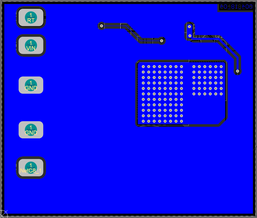
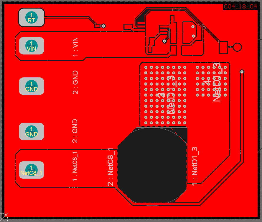
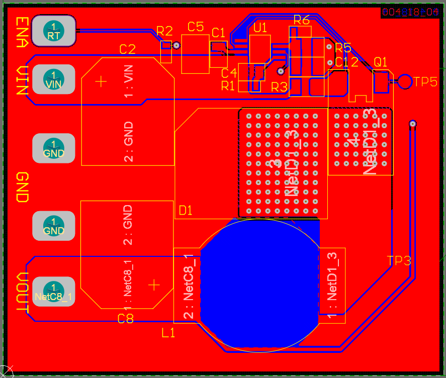
In my last post: LM508 does not work for V_INPUT below 35VDC I had problems with EMIs for IOUT >5A. I've modified the layout by moving the controller far from the position of the SW node and at the same time I've reduced the area of the SW node as much as possible. 

By doing this I've achieved to have uo to 7A at the outpout. However, for higher values my DCDC starts to work erraticaly, tha PWM frequency decays up to 20-30kHz, VOUT is 0.72V and the output current is 6.5A  when my DC-Load is configured at 10A. I really believe that I stilll having EMIs issues, I've attched my layout. 

I plan to increase the number of layers up to 4 and to place GND vias close the edge of the PCB, do you think with both I'll have enough to reduce the EMIs drastically? 

Many thanks!

David

  • Hello,

    Thank you for sharing your layout. I will reach out to the product expert to review your layout again.

    Best Regards,
    Katelyn Wiggenhon
  • David,

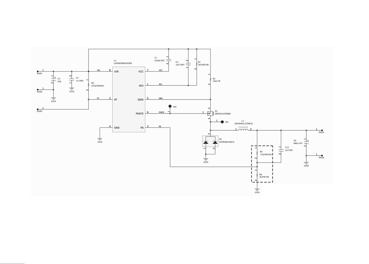
    Good to hear from you. Can you please attach an updated schematic as well?

    Thanks,
    -Sam
  • Hi,

    This's the new schematic.

    David

  • David,

    Thanks for sharing. The layout looks better but there are still a few bits that concern me.

    1. C5 negative terminal connects to the GND plane above the VIN trace but that means current must flow around the board to get to where it needs to go. This cap could connect the negative terminal to the GND plane below the VIN trace.

    2. The VIN trace chokes down to a thin trace just below R1. This should be much thicker if you want 10A out.

    3. R3 will only be able to handle 10A. Make sure you have enough margin.

    4. The trace from VOUT to R5/C12 runs along SW and directly under the gate drive signal. This is a low-impedance trace since it's connected to a big cap (C8) but C8 has lots of ESR and that VOUT->R5/C12 trace is long. It would be better if that trace was farther from these noisy nodes.

    5. The bottom layer has a large SW plane. This will help dissipate heat but it will cause major issues if you have conducted/radiated EMI tests.

    6. The bottom layer has a large GND plane (good) but it's only connected to the GND terminals. It would be good to have some via stitching so that GND plane doesn't become an antenna. Especially place a via at the IC's GND pin.

    7. There are some very thin traces (ENA, PGATE, ISEN). These should be thicker, especially PGATE. Make them as thick as the VOUT->R5/C12 trace.

    -Sam