This thread has been locked.

If you have a related question, please click the "Ask a related question" button in the top right corner. The newly created question will be automatically linked to this question.

TPS55165-Q1: Unable to get regulated output into 1K ohm load

Part Number: TPS55165-Q1

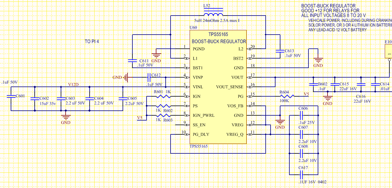
   I've got the TPS55165 on a PCB. Input range will be 8 to 18 V.  Output voltage 12V,  current needed is 320 mA max, 120mA typical. 2 sided board, bottom is ground plane. All cap values as per the data sheet. When I turn it on, I get anything from 3 to 10 volts out. Sometimes I have to change the input voltage up and down before it gets to 10V. I increased the caps on VREG up to 6.8 uF with 3 ceramic caps and 2 x.1 uF. Output C is 2 x 22uF with a .01 and .1uF.  Input C is 2x2.2uF, a 15 uF tantalum, a .1 and a .01uF.  IGN is high, PS and IGN_PWRL are low. PG_DLY goes to ground (tried to VREG, no change). Sometimes on power up PG is high (100K to +5 Pull up), sometimes it stays low. The layout is similar to the one shown, it's all very tight with a ground plane.

   Bottom line, I can not get it to output 12V under any condition. Any ideas on what to check? If not, I'll try some different part since I can't risk something this fussy in a production environment.

  The data sheet is not the best I've seen from TI. I'm not sure what is meant by the IGN_PWRL being called the "latch". I've going by section 8.4.3 and figure 16 in the data sheet which imply that you can just pull up IGN (I have 1K to +5) and ground PS and IGN_PWRL.  I just want it to turn on and stay on (no low power) on power up. What ever I use next, I'll cut a test board first (this is on the first proto of the entire system). It really should be as simple as put on the passives and get 12V out.

  • Hi Peter,

    Please attached the sch and the pcb layout. Or its hard to determine.

  • Here is the schematic and PCB layout. The ground plane is on the bottom of the PCB.

  • Dear Sir,

    The layout is very poor. there's many pin very sensitive, like  the VOUT_SENSE pin. And many trace is too thin. The power GND at the input cap and the output cap connects to the IC only with one small via, which will cause high impedance on the trace, and cause big noise.

    Please change the layout according to the example layout on page 36. Or you can also refer to the TPS55165 EVM board.

  • I'm not sure I follow your comments. There are 4 vias for the input caps to ground, two are less than .25" from the part. And on the output, there are the .01 and .1 connected directly, then the larger bulk just .35" away.
    While on the output the placement of ground and Vout is good, on the input side the pin 1 ground pin is in a really bad place for good input bypassing. If the placement is that critical, the pin-out should work with you. The fine pitch part also makes it difficult to have large traces.
    The picture of the layout in the data sheet is hard to follow, and the manual for the evaluation board shows placement but is missing a clear top foil layer. My trace width and clearance minimums are 10 mils.
    I need a solution for a double sided board with all parts on the top. While this may be a fine part, I think it's too fussy about the placement and the pin locations don't support a clean solution.
    Thank you for your response. I like the concept of the part and how it work- the micro on it, the spread spectrum the reset output. I'm reluctant to use a part that require one exact placement scheme. Perhaps a next generation part will be easier to work with. For now, I'l need to find another solution, try it on a small test board (this was cut on the final product board), and then do another big proto.
    A nice part, but not good for a 2 layer board with all connections on the top with the constraint that parts must be less than 100 mils away from the chip.
    No further reply expected, and again thanks for your help.
  • Dear Peter,

    Actually the layout Is not tricky if follow the datasheet. Input cap or output cap connect the IC with only 2-4 vias  is much less than needed. I attached a clear picture of how the component connected.

    it 'be better pour a big copper plane at the top layer make them directly connected.  Please check the below picture: