Other Parts Discussed in Thread: LMR23630
Hello TI,
we are developing a telematics device. In order to save space, I was wondering if we could place the LMR23630-Q1 and the related external components on the BOTTOM layer instead of the TOP component layer.
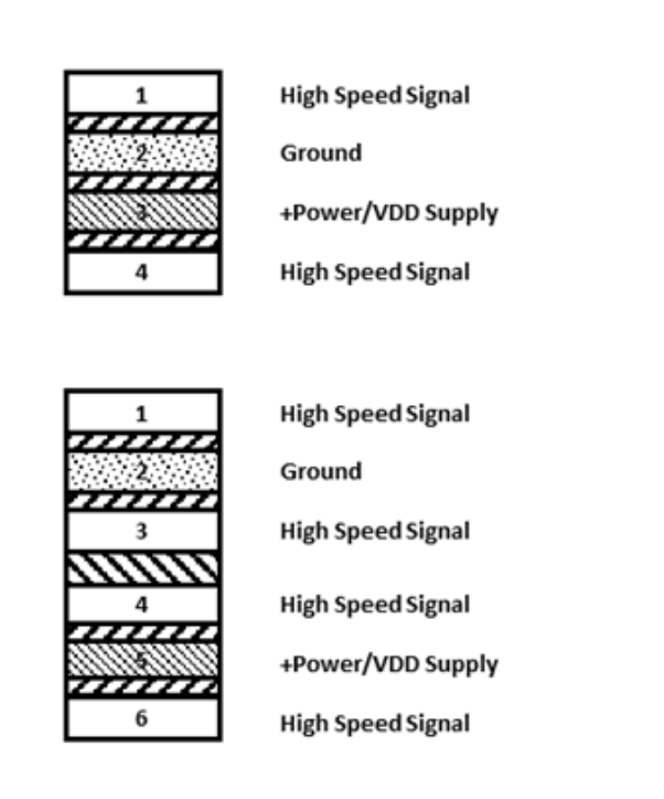
We are considering either of the following stack ups shown at the bottom of this post, depending on our signal density either a 4 or 6 layer board.
The idea is to have the RF components on the top layer and the DC DC convertors and other non RF components on the bottom layer, hopefully also reducing board area in the process.
1. What does it mean to the switching signals that would have the VCC plane as reference plane instead of a GND?
2. Should additional capacitors be placed to enable the return current to follow from the VCC plane to GND?
3. Will I be able to use the TOP side for other non RF components?
Is this even worth the effort to save space on the board?