This thread has been locked.

If you have a related question, please click the "Ask a related question" button in the top right corner. The newly created question will be automatically linked to this question.

BQ76PL455A-Q1: Multiple devices on the same PCB non-stacked

Part Number: BQ76PL455A-Q1
Other Parts Discussed in Thread: INA148

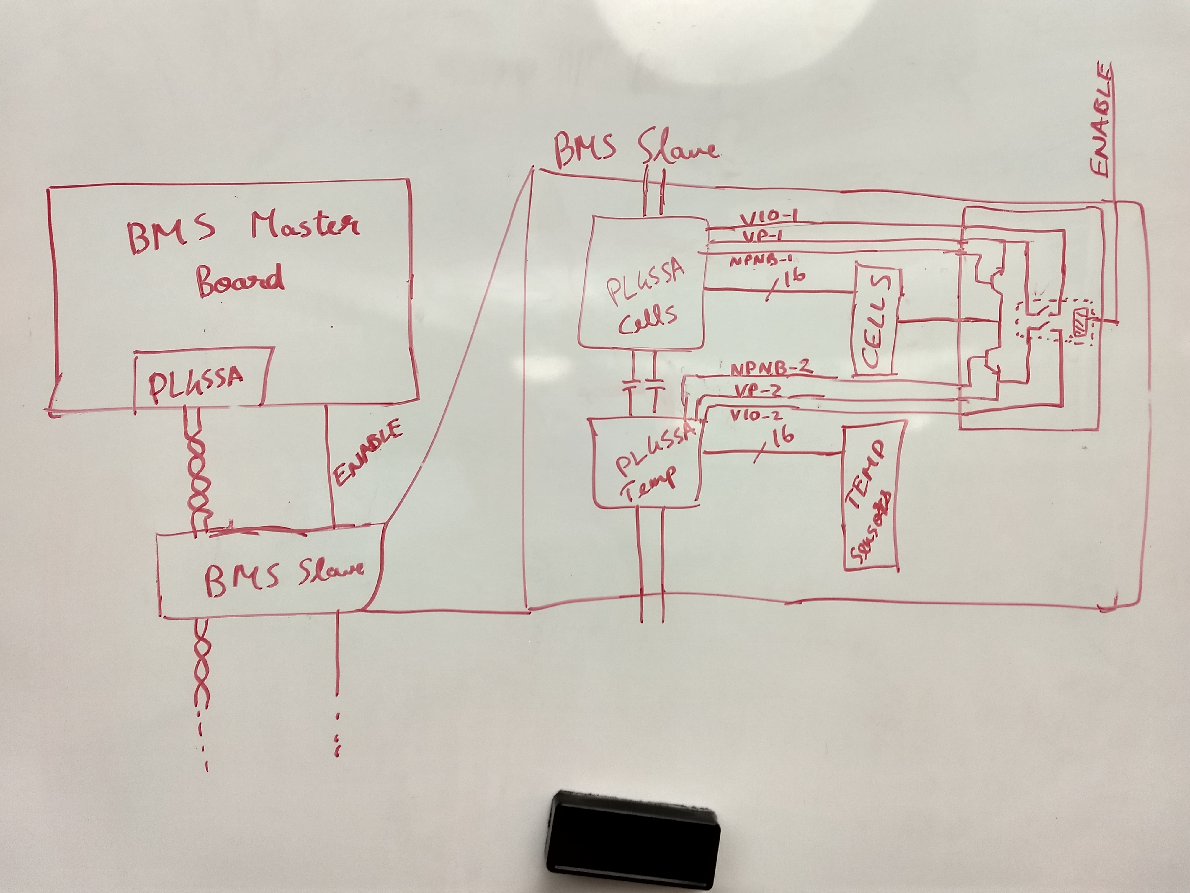
Since my application requires all 16 cell temperatures, I want to use the second device to measure cell temperature. The image below briefly explains how I plan to achieve this. 

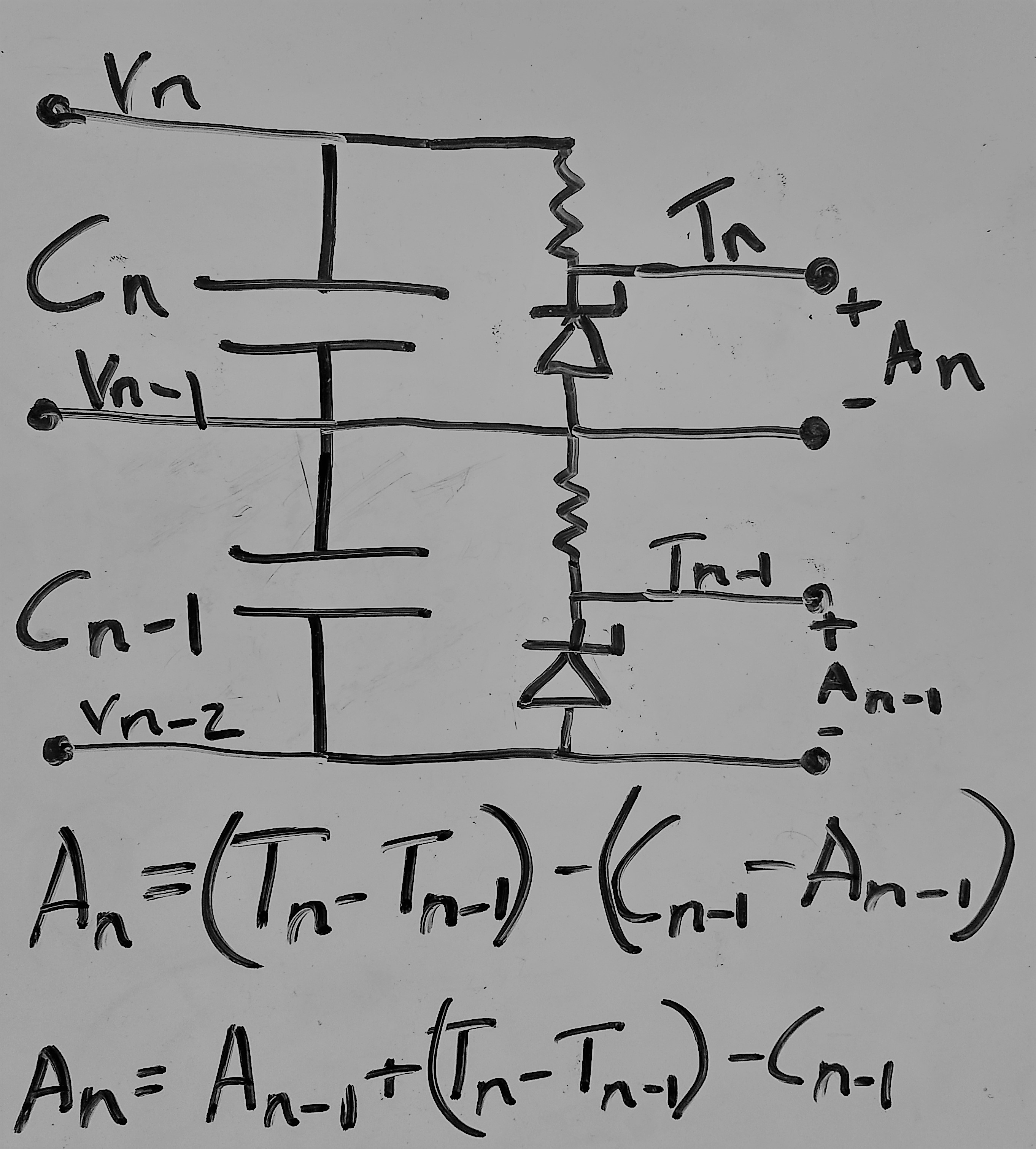
The temperature sensor is a temperature controlled voltage shunt(a zener diode with zener voltage proportional to the temperature) shown in the drawing as a simple diode due to lack of creativity. Cn is the voltage sense inputs to device1, the primary cell voltage measurement device. Tn is the inputs to device2 which is used to measure the temperature sensors' voltages. An is the actual voltage across the temperature sensor(the one with a diode for a symbol).

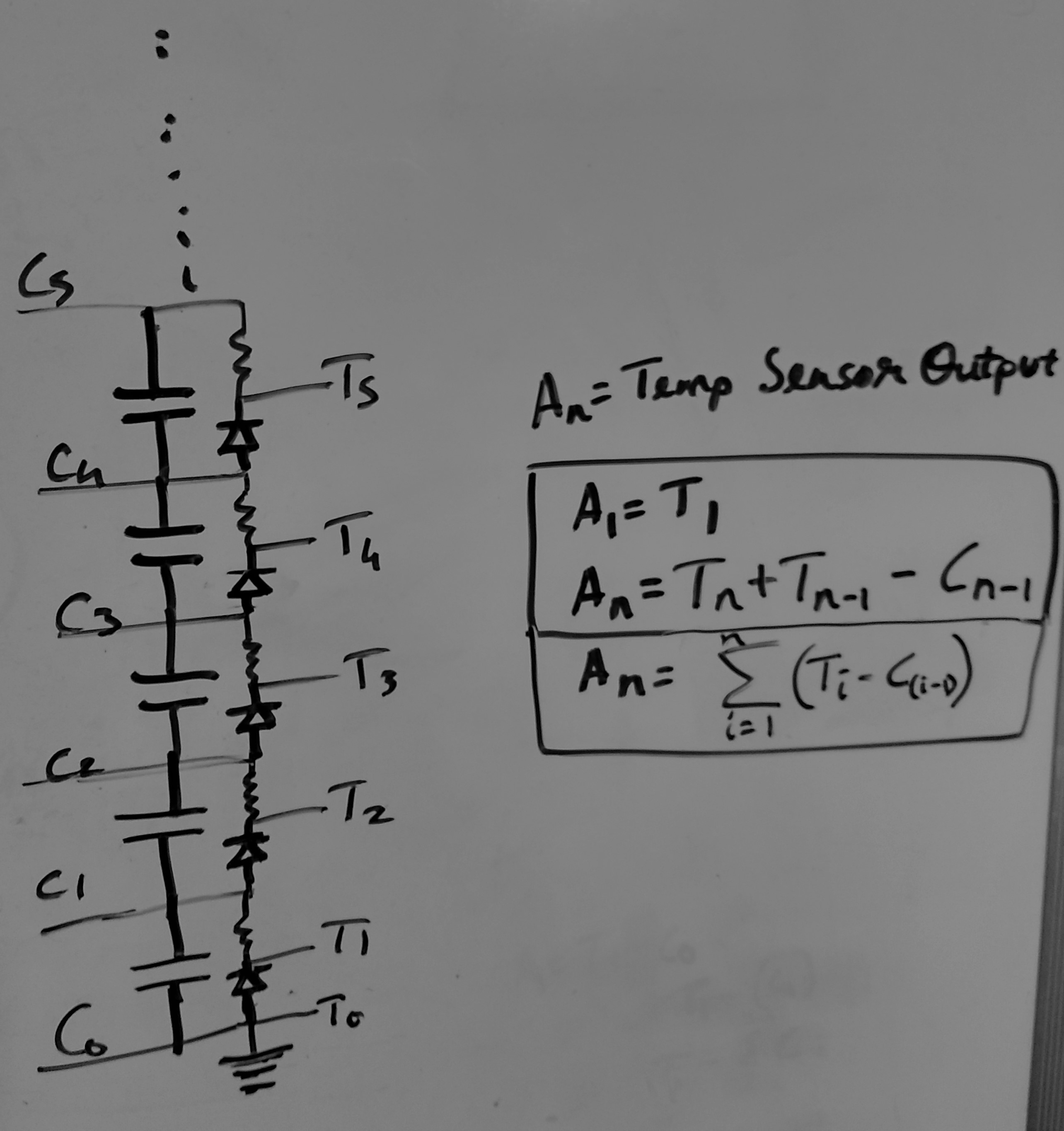
This configuration allows me to measure all temperature sensors with minimal additional cost, and fewer components on the board. The precision of the temperature measurements is up to 16x worse, but for my temperature sensors, that corresponds to <1C, which is sufficient for me.

However, this raises some issues, should I provide separate power supplies to each chip? I will be removing VIO to cause the chips to enter SHUTDOWN mode. And use a WAKEUP command over differential comms to turn them back on. VIO is supplied from VP, but a relay in series is used to connect/disconnect it, allowing externally hardware controlled shutdown of the devices as required by my application. Having one of the devices (for example, device1) controlling the NPN power supply, might unexpectedly remove VP and VDIG power to device2 if device1 enters SHUTDOWN sooner after VP power is lost. Is this acceptable?

This question is more of a clarification. If I use a single NPN power supply, the NPN controller (device1 using the case assumed above), would have to be the lower device in the communication stack right? This would allow it to receive the WAKEUP command first, and generate VP before device2 above it turns on. Will this work at all? Would the VP rise time be longer than the propagation delay through device1 to device2 and the subsequent powerup of device2 that isn't configured to control the NPN supply? Maybe this is answered in the datasheet, but I was unable to find it. 

Are there any other issues that I might have missed when using these devices in this manner? Especially since this is far from the use case described in the datasheet.

Thanks in Advance

Regards

Chaitanya

Electrical Captain

Illini Formula Electric

illiniformulaelectric.com

  • HI Sindagi,

    Do you think you can draw whole system block diagram?
    I am bit lost here.
    You don't have to be detail but I want to see how you want to connect device 1 and device 2 for 16 temp.
  • I am not sure why my reply is still undergoing moderation, I shall attempt to reply again.

    Below is a more detailed diagram/schematic of the system I am planning

    "Protection" - just the back-to-back signal diodes and resistor described in the datasheet along with ESD protection

    "AFE" - Balance circuitry and input filters for the cells

    "VSn" - VSENSEn inputs to the pl455(device1), EQn outputs go to the AFE to control discharge, however, it hasn't been shown

    "Tn" - VSENSEn inputs to the pl455(device2) for temperature measurement using the method in the original post, EQn outputs for device2 are not used

    The simplified circuit at the top is the power delivery circuit controlled by a single device that I am proposing. 

    I will attempt to create a flowchart block diagram describing the SHUTDOWN/WAKEUP procedure and post it as soon as I can, but I shall describe it in words here. The switch labeled "relay" is the externally controlled relay that will be used to cause the boards to enter SHUTDOWN when opened. To resume, the relay is first closed, returning VIO power, and then the WAKEUP command is sent over the differential communication line to turn on each device. 

    I realized I had another question, what if anything would happen if I connected the base of the NPN transistor to NPNB on both device1 and device2 using 2 diodes to prevent reverse current? This would allow either or both devices to drive the transistor and supply both circuits. This is all in an attempt to save board area, however, if this isn't feasible, I assume separate power supplies would be the feasible and fool-proof solution?

    Thanks and Regards

    Chaitanya

  • There seems to be a word limit on maximum number of words I can enter before a reply undergoes moderation, please find below my decription of the labels in the second image.

    "Protection" - just the back-to-back signal diodes and resistor described in the datasheet along with ESD protection

    "AFE" - Balance circuitry and input filters for the cells

    "VSn" - VSENSEn inputs to the pl455(device1), EQn outputs go to the AFE to control discharge, however, it hasn't been shown

    "Tn" - VSENSEn inputs to the pl455(device2) for temperature measurement using the method in the original post, EQn outputs for device2 are not used

    I apologise for all the inconvenience caused

    Chaitanya
  • HI Chattianya,
    Basically, you want to use Vsn of IC2 to measure 16 temperatures.
    Am I right?

    if I am right then show me the thermistor circuit.
    Vsn measurement is differential not single ended.

    if that's the purpose then I would end a mux rather than adding 2nd PL455A.
    Or, use 8 GPIO from IC1 and another 8 from IC2.
  • Below is the circuit and the formula I would use to calculate the voltage across each sensor. As mentioned in the original post, the temperature sensors are actually a proprietary technology which behaves like a zener diode with zener voltage varying with temperature, PFA  a datasheet that has all additional details. 

    A_n is the temperature I'd like the measure, ie, the differential voltage across the sensor(I used a zener diode symbol because I'm not sure what the standard symbol for such a sensor would be)

    V_n, V_n-1 and V_n-2 are the voltage sense inputs to IC1

    T_n and T_n-1 are the voltage sense inputs to IC2

    I did originally have a mux, but I'd also need to have high-voltage difference amplifiers(INA148) to remove the common mode voltage so that the 0-5V AUX inputs can measure them. Additional mux(es) would also be required to enable reading all 16 cells if I only had a single pl455. 16 INA148s is prohibitively expensive and an additional pl455 would be much cheaper and reduce BOM count which also lowers assembly time and costs. 

    Would the power supply design shown in the previous post work? I am concerned about powering 2 pl455s from the same power supply and how they would behave w.r.t resuming from SHUTDOWN.

    Thanks

    Chai

    Datasheet Li8P25RT revK.pdf

  • I think you have to have two separate NPN transistor.
    Because NPNB will turn off the NPN transistor.
    One device will control the power of two devices.
    Another issue is power up sequence which you need to pay attention.
    I can power two, three or many evms with 1PS but they have own NPN transistor.


    PL455A doesn't care about what you are measuring as long as you don't exceed abs max of Vsn pins.
  • Due to space constraints, I was hoping to use the chip(device1) that is lower in the daisy chain communication chain to control the NPN transistor. Would the device malfunction if it's power was interrupted by the other chip? I am interrupting the VIO supply to cause the device the safely shut down as it is. The hope was that device2, with its VIO supply interrupted at the same time that device1's supply was interrupted, would enter shutdown before device1 powered off the NPN transistor. Wouldn't this be possible?

    For power up, the VIO supply is returned to the chip. This is followed by the wake signal being transmitted over the daisy chain. The theory is that device1 will see the wake signal and turn the NPN supply on. It will also propagate the wake signal to the devices above it (device2), but since this would probably occur before the NPN supply is powered on, device2 stays in shutdown until VP and VDIG come up. After this, it will see the wake signal from device1 and exit SHUTDOWN. The wake signal is then propagated to the next board above it where the above process repeats. Does this logic seem acceptable?

    If not, are there other methods of supplying power to the boards? Could I use a basic linear regulator(LR8/LR12) with a 5.3V output and turn it on and off with a relay? Would abruptly interrupting power to the chips while they are still on, affect them? Will having the cells connected while the power supply is off, cause any damage to the chip?

    Also, where can I get information for what the current draw of the pl455 from VP, VDIG and VIO while active? I was only able to find the 31mA spike current at startup in the datasheet. If I could use a smaller SOT223-3 package instead of the recommended DPAK transistor, the space constraint won't be as much of an issue as well, but without knowing how much power I will be dissipating, this is a risky decision for me to take.

    Thanks in Advance

    Regards

    Chaitanya

  • I am bit confused.

    Let me ask this.

    Are you stacking two ICs?

    Your responds said "daisy chain communication chain" but your block diagram is not.

    You should not use external power to power 455A-Q1 for any stacking ICs.

    I only recommend NPN transistor but it's possible for BASE device using as communication(bridge) device.

  • I am extremely sorry for the confusion with the incomplete block diagrams. On each board, the devices will share the same GND but their communication will be through the same daisy chain. There will be 6 such boards with 16 cells each. There will be an additional communications bridge at the bottom of the daisy chain. 

    The question was whether I could place a relay between 'TOP' and the collector of the NPN BJT. This would allow me to use an external signal to turn the board on and off, one of the requirements of my application. I would not be using external power, just disconnecting the NPN from the cells, and I was wondering if that was an acceptable practice, and whether there was any defined behavior expected when the NPN is reconnected. The suggestion of using an external linear regulator was to force a consistent startup behavior by ensuring all power supplies were operational before the chip receives a WAKEUP pulse over the daisy chain. However, I will take your suggestion and use 2 separate NPN supplies, I think I have found some dual NPN packages that are sufficiently compact. 

    Hence, the only question that remains is the one about placing a relay that disconnects VIO from VP to cause the chip to enter SHUTDOWN. To exit SHUTDOWN, the relay will first be closed, connecting VIO to VP via a 1ohm resistor, and then the WAKE pulse will be sent over daisy chain. Does this seem viable? 

    I apologize again for all the incomplete information

    Regards

    Chaitanya

  • You don't need any relays. NPNB will shut off and ON the NPN transistor in Shutdown and wakeup mode.
    When you send wake signal to base device, it will wake base and daisy-chain device as well. Same as shutdown.
    Just follow our recommendation then PL455A will take care your wake and shutdown.
  • Please correct me if I am wrong, the recommended method of shutting down the pl455 is using the SHUTDOWN command sent over UART/Daisy chain right?

    This would not work for my application for 2 main reasons.
    Firstly, when the vehicle is turned off, the power is cut with no warning or preceding signal. This would cause the microcontroller connected over UART to the communications to power off before it could send a message to the daisy chain, asking all the pl455s to enter SHUTDOWN.
    Secondly, if I were to use a large capacitor to power this microcontroller long enough to allow it to send the SHUTDOWN message, this would rely on the communications over daisy chain to be faultless. It would not be acceptable in my application for a section of the pl455s to not shutdown due to not receiving the SHUTDOWN command because of a loose crimp, broken trace, improperly seated connector, or any other multitude of hardware or software issues.

    Having a relay that is directly powered off an external source(for example, the vehicle's electrical system's 12V supply), and is configured to be normally open, would force all the connections and appropriate switches to be turned on before the BMS can exit SHUTDOWN state. Moreover, when the central 12V supply is turned off, this relay would return to its normally open state, interrupting the flow of current from VP to VIO, causing the VIO voltage to fall below threshold and force the pl455 into SHUTDOWN.

    Is this not an appropriate and/or efficient method to ensuring an external supply can WAKEUP/SHUTDOWN the entire pl455 stack instantaneuosly?
  • Do you think you can provide block diagram of your system?

    If not comfortable then you can send it to me privately.

  • I'm not entirely sure what a block diagram is in the way that you would prefer. Below is a diagram that covers the entire system's power supply functionalities. The idea is to use the BMS master board's enable output signal to turn on and off the entire stack of slave boards