This thread has been locked.

If you have a related question, please click the "Ask a related question" button in the top right corner. The newly created question will be automatically linked to this question.

LM34910: Power supply fails if we use alternate components

Part Number: LM34910

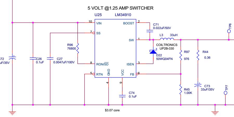
We have been into production for years with a board having LM34910 as one of the regulators. This is the main supply (logic circuits, 5V) of the board. The board has a microcontroller and a series of opto-sensors. The total power consumption (which is almost steady) is about 250mA. As the board was designed by a third party consultant at the time, we do not know the design parameters they used to. In the past a research on a similar board revealed that the values of the main inductor and the output capacitor were not the best solution and we believe this could be the case in this board as well. Nevertheless we have produced these boards in the past (around 15K) without a problem.

Here is the original circuit:

Recently out assembly manufacturer needed to add alternate components as the original parts specified were hard to find or were obsolete. It seems that after a point some of the boards (10 out off 1000) fail to communicate if we connect all or part of the load (opto-sensors), as a result of instantaneous under-voltage when the microcontroller tries to activate through a FET the LED power.  

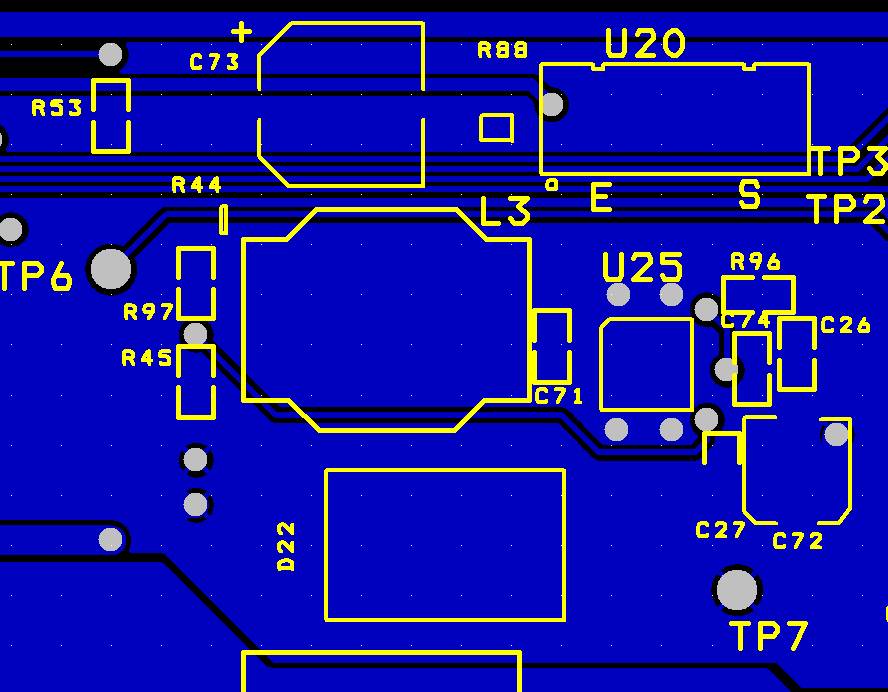
The parts replaced are D22 and L3.

Part Designator Original Component P/N New Component P/N
L3 Eaton/Bussman, UP2B-330-R Coilcraft, DO3316T-333MLD
D22 Vishay, VS-50WQ04FNTR-M3 Diodes Inc, SBRT10U60D1-13

Our manufacturer says that the L3 tolerances are such that a higher inductance make the boards fail. As a proof he used a part with less inductance for L3 (27uH) and made these boards work.

However a colleague of mine, used the old D22 part instead (with the new 33uH inductor) and fixed his boards as well. 

We have also noticed that heating the boards (after soldering task etc) makes the boards working until they cool down, where they start failing again.

Also if we start removing the loads (opto-sensors) one by one the boards become operational again.

It seems that the circuit is affected by the load (which is how we identified the problem, initially).

In order to check things myself, I measured the circuit with my scope at Pin 1 of the regulator on a good working board from the past (ie. original components). The regulator seems to work in continuous mode at 454KHz (as set by R96). However the pulse shows some ringing:

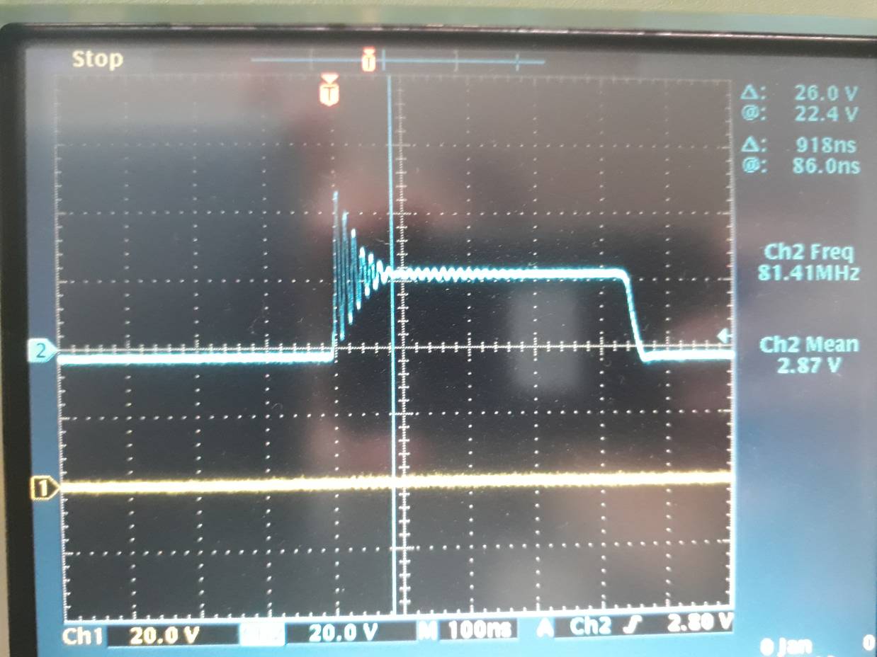
Good board, Output of Switcher.

I then instructed my colleague (I do not have direct access, this is in another location) to measure the same point on a failing board:

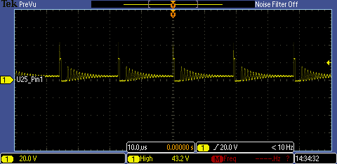
Bad board - not working, output switcher

It seems that the switcher works in a non-continuous mode (at about 60KHz).

Also note that after the pulse is finished (the small rectangular peak in the scope) the output voltage is 0. Later on a ringing happens and increase this level to 5V that remains till the next pulse.

It seems that the diode plays a critical role in this and the only obvious difference might be the Vf level of the diodes, as checking the plots seem to have 100mV difference.

Can you please explain how the diodes can affect the circuit and which parameters are critical?

As you may understand the boards are already manufactured and the best remedy is to change as few parts as possible. Our manufacturer proposes a slightly lower value inductor, but we have seen that the diode may also fix the issue. What is your recommendation?

Thanks in advance,

Ilias

  • Hi Ilias,

    For the diode the two most important parameters are reverse recovery time and forward voltage. The forward voltage should be approximately 0.75V in order to protect the device during current limit or overload operation. This voltage will force the inductor current to reduce.

    I see you have noted on the schematic 1.25A load. Is this the load condition that you are seeing the failures at? What is the input voltage range that you are seeing the failures as well?

    Thanks,
    Katelyn
  • Hi Katelyn,

    the input voltage is constant at 24Vdc.

    The load starts with around 80mA and then tries to jump to 250mA normally due to the sensor activation early in the reset routine of the microcontroller.

    One other difference we notes is that the regulator was also changed from LM34910 to LM34910C. Could this be an issue?

    The 1.25A is stated in the schematic, but I am not sure if this value was used for the calculation of the L/C network. Unfortunately we don't have any documentation on the design of this power supply units.

    Regarding the first scope plot I had provided on a working board, is this ringing expected (and acceptable)?
  • Hello,

    I do not expect the change from LM34910 to LM34910C to cause the issue.

    This is a significant amount of ringing. Are you using a tip and barrel method for this measurement? Could you share the layout for this device? One possibility is that the parasitics of the new components has shifted from the original components. You do not want the absolute maximum to be violated on the VIN or SW pin for any period of time.

    Best Regards,
    Katelyn
  • Dear Katelyn,

    No I did not use the tip and barrel method in this measurement, as I would need to modify the board (to get a ground point near the D22 cathode measurement).

    I also discovered that measuring the same node on a different component (close to LM34910, pin 1 and the inductor) this ringing was 5V lower (peak value) than what I saw in D22 cathode.

    The back side of the D22 (anode) had a much smaller amount of ringing which makes me believe the ringing is real.

    I have also used the same method to check another board, which I have designed myself with LM22676MRE-ADJ and there is no ringing at all at the switcher, indicating probably that the ringing shown here is valid. Also note how clean is the falling edge of the pulse, without any noise/oscillations either. 

    And this is a working circuit.

    Please check the layout as well:

    Top Layer

    Bottom Layer

    Thanks,

    Ilias

  • Dear Katelyn
    In order to make things easier, we did continuously activated the load (so it is always stable and not controlled by the microcontroller).
    A failing board will not be able to keep the voltage level at 5V, but rather stays at 4V. Input voltage is always 24Vdc stable.

    We discovered also that the failing part is due to the New diode.

    We have concentrated at the diode part SBRT10U60D1-13. Can you tell us why this part will make the board fail?
    From the specifications it seems a similar device with the original part, VS-50WQ04FNTR-M3.
    Recovery time is not mentioned in the datasheet as this is not defined for Schottky diodes; Capacitance is about 100pF different.

    Thanks,
    Ilias

  • Hi Ilias,

    These two documents discuss the different considerations when choosing a diode:
    www.ti.com/.../slva477b.pdf
    e2echina.ti.com/.../Efficiency-of-synchronous-versus-nonsynchronous-buck-converters.pdf

    I believe the ringing is real as well, I was just trying to understand what the true magnitude is of the ringing. Using a long ground wire will make this ringing appear greater than it is. Second, looking at your layout I would recommend moving the C26/CIN directly next to the IC.

    Also, for my understanding, when you say failing part, do you mean the part is permanently damaged or that the output voltage is lower than expected (4V)?

    Thanks,
    Katelyn
  • Dear Katelyn,

    When I say failing part, I mean the power supply fail (voltage below 4.85V, most commonly 4V or less). The part is not broken.

    We have selected and experimenting with the following diode from ON Semi: MBRD360T4GOSTR-ND , with good results.

    Regarding the ringing: I managed to use the tip-barrel method.

     1. With minimum load (0.2A), ringing span is 14Vpp, max voltage 38V.

     2. With 0.8A (our normal max is around 0.3-0.4A) the board failed with 1.4V output. At the same time I got a ringing span of 44Vpp, max voltage 52V. 

    So the initial photo with ringing (and the relevant levels) is correct.

    Another experiment was to start reducing input voltage while having a load, to see in which voltage input ranges the power supply failed.

    With the above load (6.8 Ohms), I started decreasing the input voltage. The board started working (aka delivering 5V) in the 8V-22V range. At 22V the maximum peak voltage was 50V at the switcher/diode.

    I guess the problem is due to the ringing and the maximum voltage levels achieved on the switcher and the diode.

    The ringing should be a PCB issue. I see the feedback line crossing and splitting the ground on the bottom layer, just above the diode is. 

    Thanks,

    Ilias

  • Hi Ilias,

    Thank you for your help clarifying your issue.

    Yes, I agree that the ringing should be a PCB issue. This can be made worse by different component choices because ringing will vary based on the specific parasitics of both the PCB and components. The On Semi diode looks like it could be a good choice. I am happy to hear this diode is working out for you.

    If you were to do a PCB spin, I would recommend choosing smaller package sizes for the inductor and diode in order to shrink this loop. Also, I would consider using a ceramic output capacitor to decrease this loop as well.

    Also, you are correct that you never want the FB trace to cross the SW plane.

    Best Regards,
    Katelyn