This thread has been locked.

If you have a related question, please click the "Ask a related question" button in the top right corner. The newly created question will be automatically linked to this question.

PMP8740

Other Parts Discussed in Thread: PMP8740, UCC28950

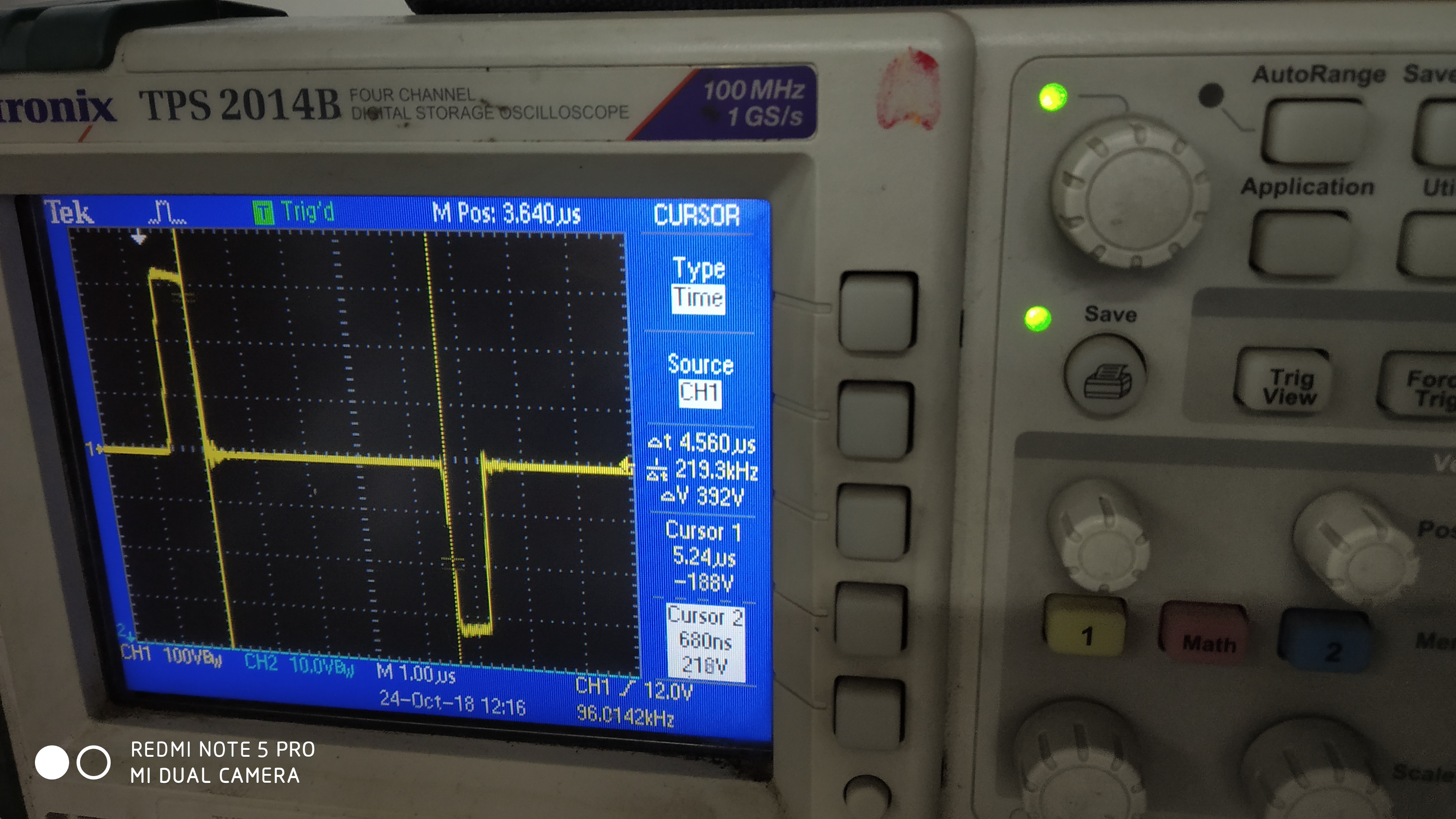
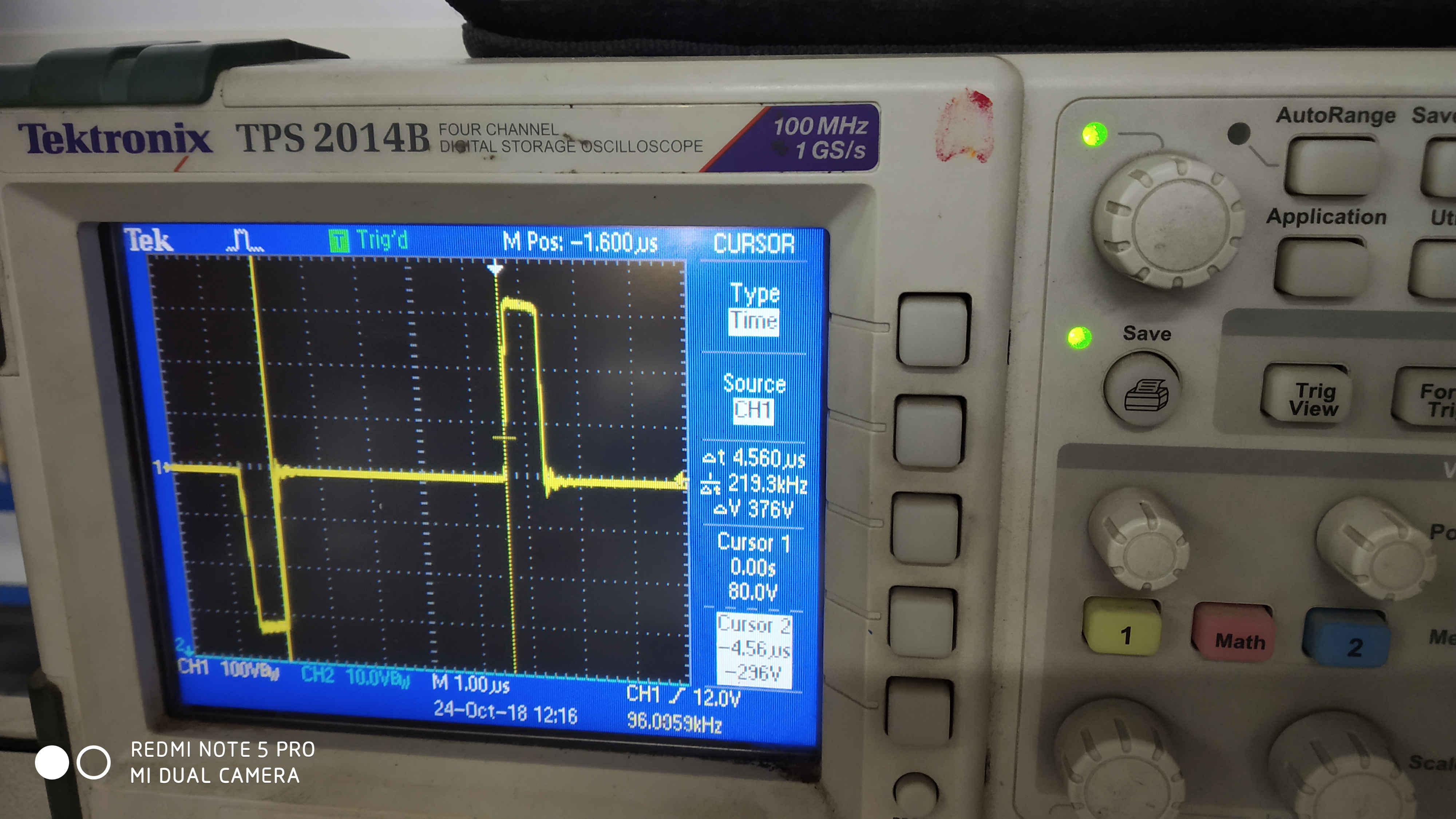
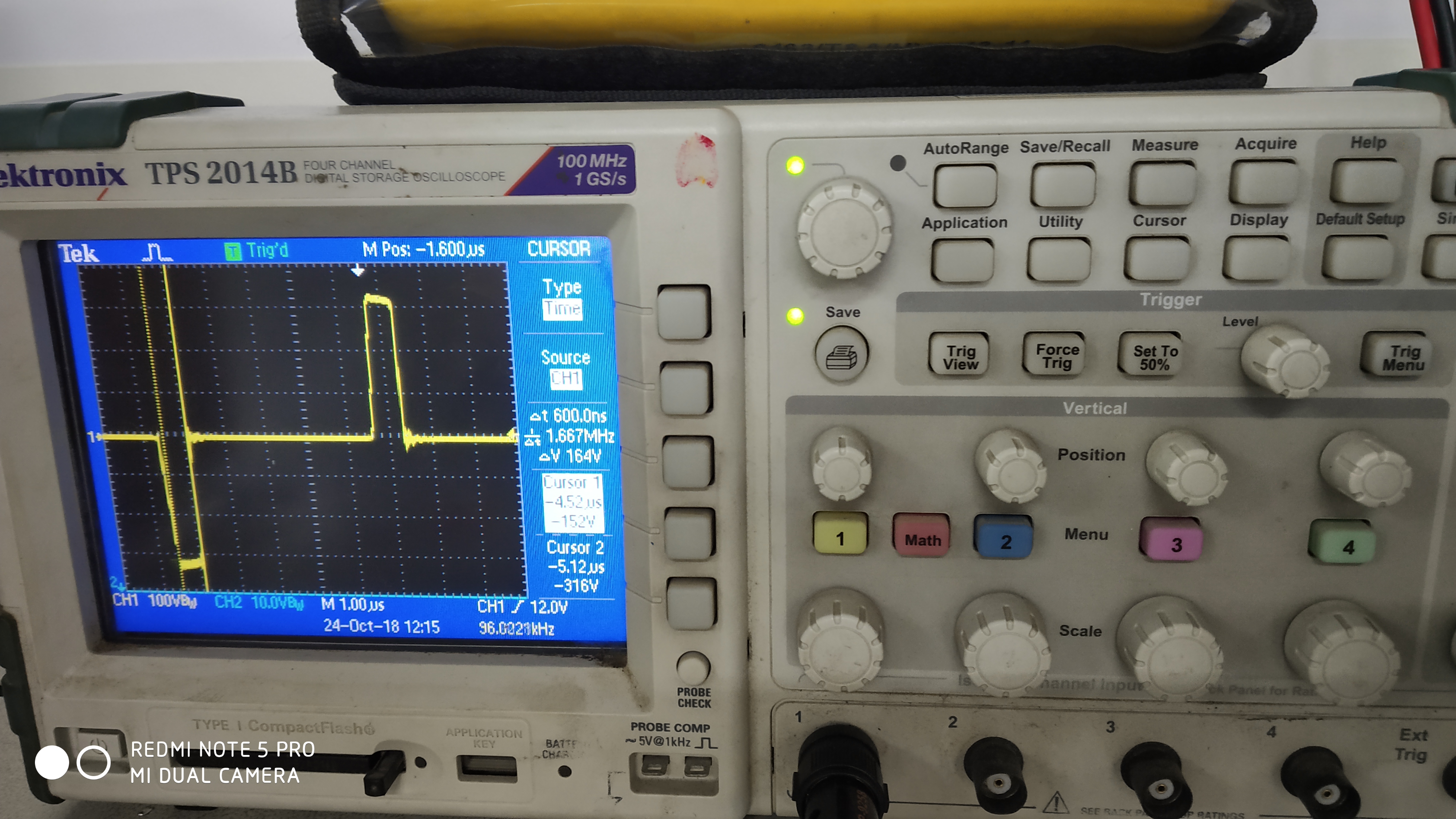
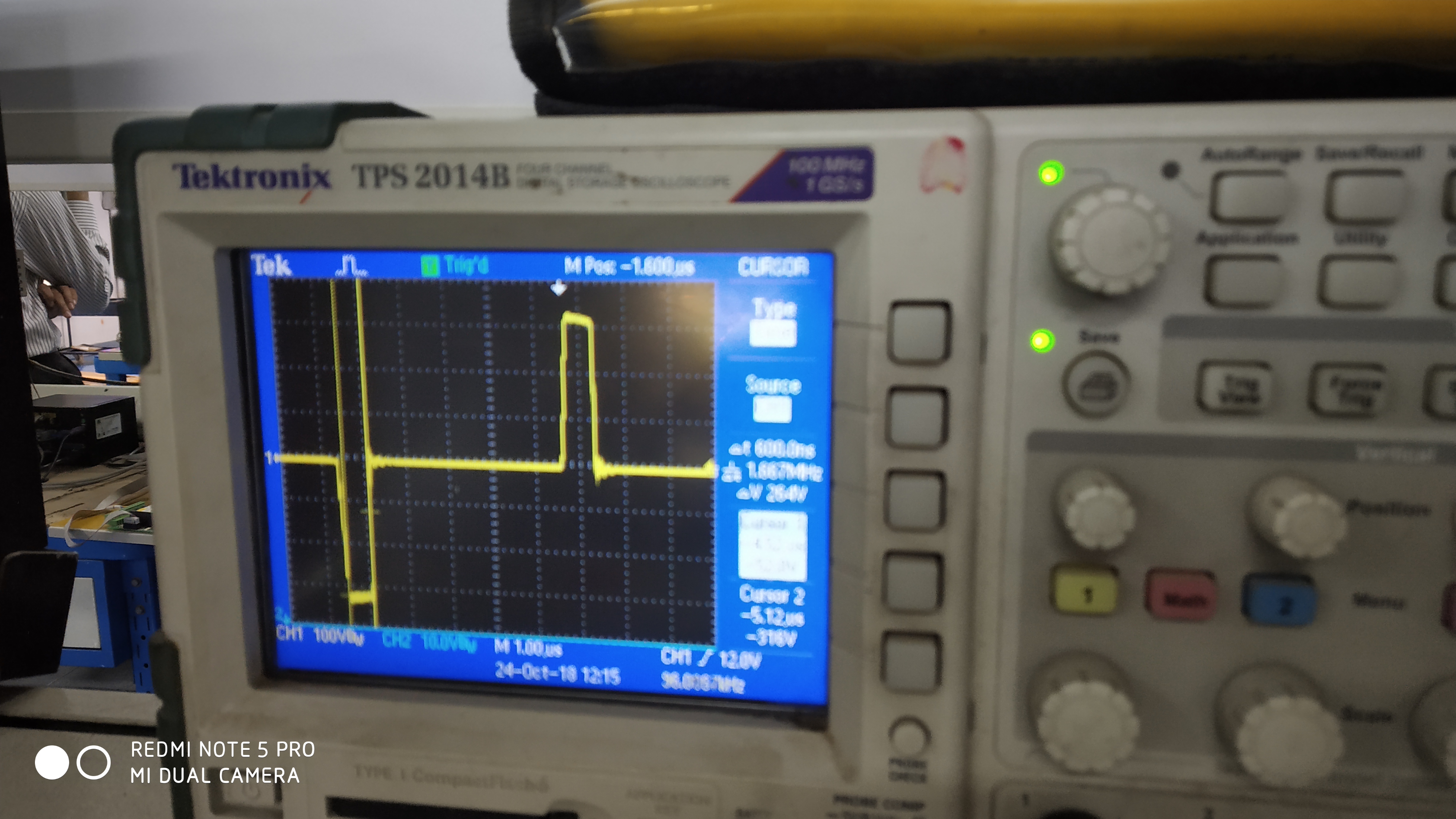
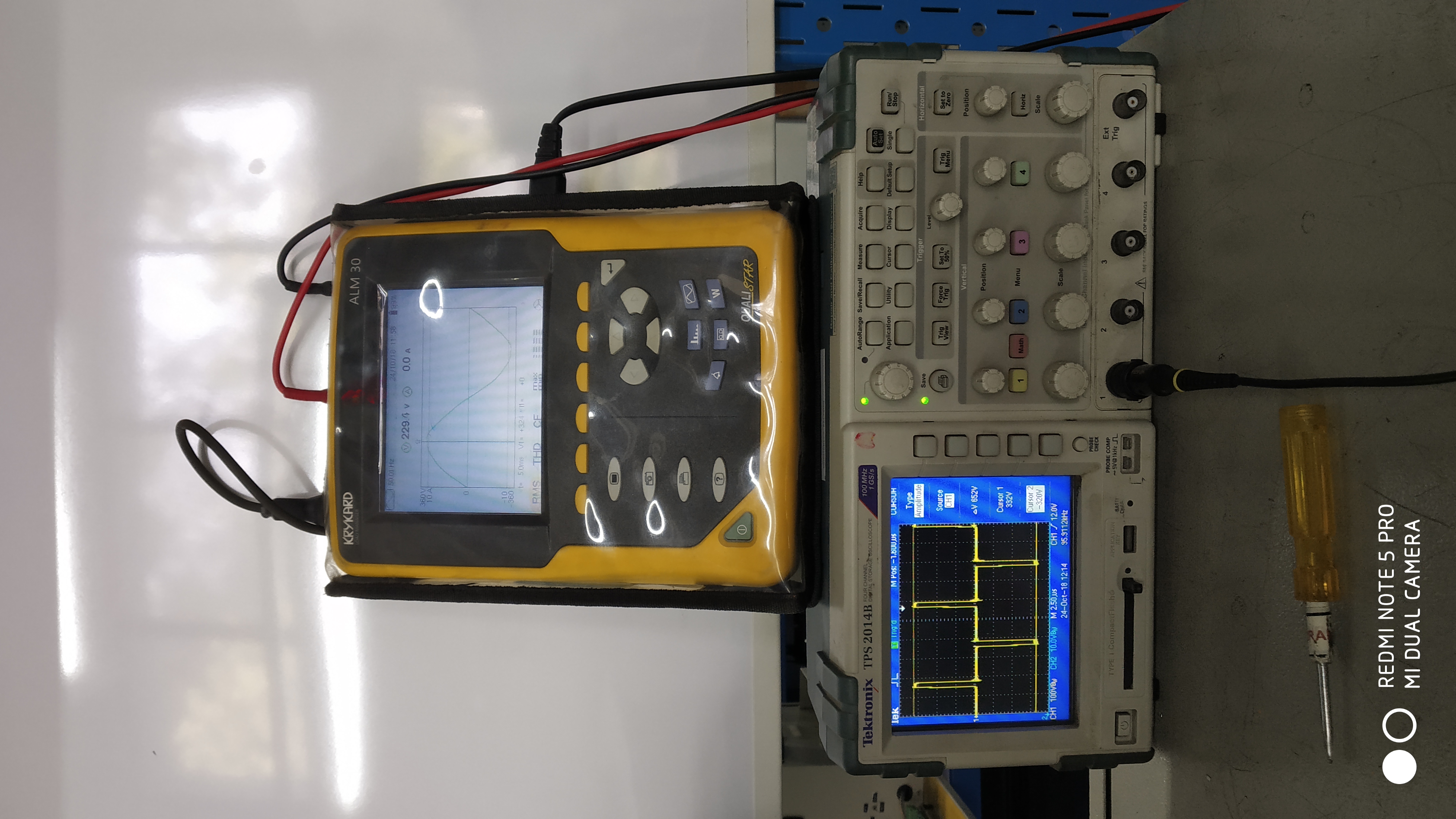
Correct.. . today i tested DCDC at no load and power-up through rectifier+ 330uF/450V capacitor. I am attacheing waveforms of transformer primary at no load.  also i got stable output voltage of 53.9V at output of DCDC converter.  After this i tried to load 1.5A current (37.5Ohm Resistive load) but output get reduced to 3V -1.5V , but if i disconnect the load then output voltage recovered to 53.9VDC. 

Is this because of my voltage control loop?

My transformer is  PQ50/50, Primary1: 8Turns, Secondary1: 3Turns, Secondary2: 3Turns, Primary2: 7Turns .

Thanks, 

Anjana

  • Also, is it necessary to populate R4 (100K) On DCDC board? because my system is standalone battery charger.

    Anjana
  • Dear Anjana,

    I believe you are right. The converter works to supply the maximum output voltage possible, but runs in DCM, therefore at no load you have 53.9V.

    Please reduce the voltage on the reference pin (U1A, pin 3) for example at half the nominal voltage (if you have here 2V, then put a 100 KOhm resistor in parallel to R29 and you should have ~ 1.23V. Check that the output voltage of the converter is reduced. If this doesn't happen, please check the way you close the loop (D1, EA+ voltage on U2 etc.)

    Best regards,

    Roberto

  • No, R4 is not needed as stand alone battery charger.
    Thanks,
    Roberto
  • Dear Roberto, 

    1) what will happened if i reduce U1pin3 voltage to 1.23V?

    2) As mentioned in Datasheet,  DCM  mode starts when the voltage at CS pin is lower than the threshold set by user, in this case it brought down OUTE and OUTF signals to zero. So my doubt is , as my DCM threshold voltage (i.e. Voltage at DCM pin) is 0.22v and i am loading 1.5A current, the controller enters into DCM mode and turns off SR pulses and hence output voltage drops down to 3V.

    3)So to work properly i should load min. 5.5A current, because as per VRS formula given in datasheet i calculates as below...

    VRS=((((2000*0.15)/54) +(7.41/2))*12ohm)/(5*100)

           =(5.55+3.705)*12/500

          =0.22V

    RDCM (R18)=1K and RDCMHI (R7)=22.1K selected

    Also if i want to load 1A minimum current i should calculate like this .... ((1*0.15)+3.705)*12/500= 0.09252V VRS and RDCM (R18)=1K and RDCMHI (R7)=53K 

    is it correct. 

    Thanks, 

    Anjana

  • Another thing, Why synchronous rectifier pulses depend on CS pin voltage ? because CS pin senses input current of DCDC stage.

    Anjana
  • Dear Anjana,
    All converters with sync-rectification FETs work also without driving them. In fact, if there is no driving pulse on their gate, the internal body diode will act as a normal rectifier, therefore also your full bridge must work without driving the sync-FETs. Of course, at higher currents (typically in a range of 5%...20% of nominal load), you should set the DCM threshold so that they become active, otherwise the Vf of the body diode is creating too much losses (and you have to take into account that these body diodes are very slow, so you get also high current spikes and switching losses).
    So, to recap, set DCM level according to your needs (I typically set it to 0.75...1 * peak-peak worst case ripple current on the output inductor).
    Best regards,
    Roberto
  • As soon as the CS pin voltage (which is proportional to output peak inductor current, divided by turns ratio of the transformer) reaches the voltage set to DCM pin, the sync-FET pulses become active, to avoid high conduction and switching losses in body-diodes.
    Thanks,
    Roberto
  • Dear Roberto, 

    Dear Roberto, 

    Thanks for reply.

    But sorry to say I am not getting your answer. 

    I only got that, if SR pulses are turned OFF output voltage still be there through body diodes of SR mosfets.

    As per the design sheet shared by you the calculations are like... (((1920*0.15)/32)+(7.41/2))*16.2)/(9.66*100)=0.2 and RDCMHI=15.4K and RDCM=562 Ohm.(these two resistor values used in PMP8740)

    I too calculated the DCM voltage and resistors as per your calculations. 

    How much minimum current I should load in my case?

    and finally if DCM is not the issue then what will be the reason for output voltage get down at the time of loading?

    Anjana 

  • Dear Anjana,

    I believe that the minimum load current, to get the sync-FET always on, is 20% of your nominal load.

    Anyway, if the output voltage drops with a small load, please check with an oscilloscope the voltage on R34 (of my schematic). If this voltage is too high, it might trigger the over current protection.

    Best regards,

    Roberto

  • Dear Roberto,

    yesterday at the time of testing of dcdc converter we come across one problem in frequency of gate drive pulses.

    i have given 12v external supply to control circuit only, not 400V dc.

    when i check gate drive pulses OUTA to OUTB, OUTC to OUTD i observed , at start pulses (frequency and amplitude) are as expected, power supply current also as expected. but after around 1 min frequency of pulses starts decreasing and after some time frequency get further reduced and power supply goes into current limit (more than 350mA current flows from power supply).

    Please help me to understand what is happening, and suggest any solution to overcome it.

    Thanks,

    Anjana 

  • Dear Anjana,

    Probably the power supply goes into current limit because of low frequency pulses generated by the controller U2 (UCC28950). Since this happens, the gate drive transformers T2 & T3 will saturate and draw high Vdd currents on drivers. The controller U2 should never change its switching frequency so I suspect it's an issue coming from U2 overheating. Please check with a thermometer its surface. It the temperature is too high, it might be damaged, so I suggest a replacement.

    If with a new one it still overheats, you might have one of the drivers U9 or U10 (and check also U12 and U13) damaged.

    Please let me know if that issue is solved.

    Best regards,

    Roberto

  • Dear Roberto,

    We have checked vref of 28950 it changes from 5v to 6v . Regarding to heating 28950 and all gate driver ics are not heating. So now we are replacing 28950 and will check waveforms again.

    Why this ic fails? What is  failure rate of 28950?

    Anjana

  • Dear Anjana,
    The issue might be the board layout. Please check that the net connected to Verf isn't too long or close to a switch-node. In that case, this net could capture switching noise. if so the internal Vref generator might be perturbed, drawing too much current and involving high Vdd current (and overheat). The solution is to make the Verf-net as short as possible. If you need this Vref for other functions in your power supply, plan to add an operational amplifier, set as voltage follower; this action keeps Vref decoupled from the rest of the board.
    Best regards,
    Roberto
  • The converter works to deliver the most output voltage possible, but runs in DCM, consequently at no load you have 53.9V.

    Please lessen the voltage on the reference pin (U1A, pin 3) as an example at half the nominal voltage (if you have here 2V, then placed a 100 KOhm resistor in parallel to R29 and you have to have ~ 1.23V. test that the output voltage of the converter is reduced. If this does not take place, please take a look at the way you close up the loop
  • Dear Roberto, 

    Thanks a lot for reply.

    Board layout is as per PMP8740 gerber. we have changed the 28950 ic and going to test further. Hope for best performance and throughout working of DCDC stage .

    Thanks,

    Anjana

  • Dear Roberto,
    what procedure did you followed at the time of testing of DCDC converter?

    Did you directly powered up DCDC from PFC or you also used rectifier at first to test DCDC?

    another thing. when i am testing it from rectifier, i powered up control circuitary from external 12V power supply at start only , then i increase AC voltage and looked for output voltage to be stable. is this correct. or should i follow any other procedure?

    please suggest.

    Anjana
  • Dear Anjana,

    I made the following to test the DC/DC:

    1) Supply 12V on pin 9 of J5 (VCC_FB)

    2) Short PWM_Vref P2.4 and PWM_Iref P2.3 both to ground

    3) Apply 3.3V, or the output voltage of U7 (+3V45) to Pre-Charge P2.2 net (R84) to enable back-to-back FETs Q12...Q31

    4) Short to ground the gate of Q1, or apply +3.45V to net ENA_FB P4.7 (R33)

    5) Apply a small load on the output of DC/DC converter (10 Ohm to start with)

    6) Apply Vin on J7, starting from zero and increasing to 10V...50V

    7) Watch the voltage on drain of Q15 and Q16, and also in differential on the main transformer T4

    8) Check that the output voltage of the converter fits with Vin value and turns ratio (since here the duty cycle is maximum)

    9) Increase Vin on J7 to higher value until ~ Vin(nominal)/2

    9) Put a 100 KOhm resistor is in parallel to R29, and verify that when Vin is higher than half of nominal input voltage, the converter enter regulation, by reducing the duty cycle (again, by watching the waveform across primary side of T4).

    Best regards,

    Roberto

  • regarding the second question, the procedure is correct: please consider that you will have 100Hz ripple on the output when running in open loop.
  • Dear Roberto,

    Today at the time of testing i face the same problem of reduction in output voltage. again i load 1.5A and output voltage get reduced to 3V from 53.89V. at this time i checked CT output voltage across R34, which is as below
    VinAC=220VAC, IinAC=0.81A, Iout=1.5A, Voltage Across R34=0.052V

    I used R34=12Ohm.

    is it correct? please tell me how to calculate CT output volatge.

    Thanks,
    Anjana
  • You mean i should check ripple by removing D1 & D3 diodes? open loop will increase input current right?

    Anjana
  • Dear Anjana,
    The voltage across R34 can be calculated according to the following:
    Take the output current of the power supply (for example at 1.5A). Add inductor ripple current (half of peak-peak). Multiply by main transformer turns ratio (T4). Divide by current sense transformer T1 and then multiply this current by the value of R34.
    For example, if T1 is 1:100, T4 has a ratio of 5:1, the inductor ripple is 1A peak-peak, we have :
    V(R34), peak = {[(1.5A + 0.5A)/5]/100}*12 Ohm = 48mV (which is close to the value you are measuring).
    Now, in order to understand what happens to your converter, I need to know (in the actual conditions, where you have 220VAC and 1.5A load):

    1) Voltage on pin 1, 2 and 3 of U1A.
    2) Voltage on pin 5, 6 and 7 of U1B.
    3) Voltage on TP6

    Best regards,
    Roberto
  • No, please, do not remove D1 and D3 diodes, otherwise the converter will work in open loop conditions.
  • Dear Roberto, 

    i load 4.5A current but still the situation is the simillar. 

    i am wondering is my transformer correct?

    As per my calculation primary inductance calculated as 1mH but at the time of manufacturing manufacturer told me without airgap they are not able to achieve this inductance hence with NO airgap i got 1.4mH of primary inductance. is this the reason for output voltage lowering? primary and secondary waveforms are as expected. 

    Anjana

  • Dear Anjana,

    I don't think the transformer primary inductance is affecting the regulation of Vout, unless it saturates.

    Usually, in order to get the exact magnetizing inductance and increase the saturation point, a small air gap is needed.

    You can check if your transformer is saturating by measuring (with the help of current probe) the current flowing in the primary side of the transformer.

    By the way, did you measure the voltages I listed in the last emails? Please let me know the values of those voltages and, if possible, a screenshot of the current in the primary side of the transformer.

    Best regards,

    Roberto

  • Dear Roberto, 

    1)

    we load 12ohm resistance (4.5A) at 230VAC input, we got same phenomena of output voltage comes down.  At that time on Current meter connected to output shows 1.75A instead of 4.5A. we got voltages as follow...

    at current loop (U1B)

    Iref=1.99V constant throughout

    TP6= 0.175V when load ON , I out actual on current meter = 1.75A

    Opamp pin 7= high 12V

    I used shunt (R92)=1mOhm, R93&R94=1K8, R100&R101=178K

    at no load, About voltage loop (U1A)

    Pin3=2V constant Through out

    Pin2=2.3V

    pin1= low 

    2) Regarding to transformer it is not saturating , also i had doubt on winding starts and ends but they are also correct. 

    3) when i looking in PI loop components, As per my calculations I got 227K, 0.56nF, 68pF for R3, C2, C1 resp.  i am attaching the images of bode plot for both as per my value and and as per actual values used in circuit (i used your values from pmp8740 in my PI ) 

  • Dear Anjana,
    The voltages on current loop error amplifier (U1B) are correct.
    The question is: how can you have 2.3V on pin 2 of U1A if the output voltage drops down almost to zero?
    Did you connect back D1 and D2 on the board?
    What is the voltage on pin 2 of U1A when Vout drops?
    Regarding the voltage loop, in this moment it's not very important and it will be as soon as your converter is regulating your load and is able to supply the current at the right voltage level.
    Please let me know.
    Best regards,
    Roberto
  • Dear Roberto, 

    today i tested the voltage loop voltages at loading condition. they are as follow

    Vinac=215VAC

    Iinac=0.77A

    Vout=36V

    Iout=1.5A

    U1A-pin3=2V constant

    U1A-pin2=voltage drop from 2.021 to 2.016V when loading

    U1A_pin1= low when vout reaches 53.9V  and durring loading

    2) today our output voltage not dropped to the 3V , it drops upto 36V only. we have not done any changes in the circuits. 

    and I am measuring this output voltage at J8 output connector. 

    3) after this i removed D3 diode (disconnect current loop) .... and checked the voltage loop voltages they are same as above. 

    Thanks, 

    Anjana

  • dear roberto,
    Now i checked the voltages at TP3 and J8 both are as follow

    At no load: at TP3:-54.39V & J8:- 53.87V
    At 1.5A load: at TP3:- 54.39V & J8:-6V

    So is the problem in RT1, RT2 and mosfet array circuit? what should i check there?

    Thanks,
    Anjana
  • Dear Anjana,
    I assume that when you say that the voltage on TP3 is -54.39V, you meant +54.39V, correct?
    If this is not, just consider that this power supply cannot generate negative output voltage.
    If instead you meant all positive voltages on TP3 and J8 (pin 1 is positive, while pin3 is ground), it looks like the back-to-back FETs are not driven correctly.
    Please check that, after connecting 3.45V on net Pre-Charge P2.2 (right side of R84), you measure ~ 12V on gate-source voltage of any FET (Q12...Q31).
    Best regards,
    Roberto
  • Dear Roberto,

    You are right all voltages are positive and measured w.r.t. GND-S. and On J8 i connect multimeter between J8-pin 1 and J8-pin 3

    OK i will check G to S voltage of Q12..Q31.

    Atleast today i am able to isolate the problem, now i can focus on Q12...Q31 and its driving circuit.

    one request Roberto, i will again go through the explanation of this circuit given in white paper (design review of a 2-KW parallelable power supply) but i am still not getting what is the purpose of V-float and A-D18 and pre-charge P2.2 signal. can you please explain me?

    Also, what is the purpose of to use mosfet array? because traditional way is to use series diode.

    Thanks,
  • Dear Anjana,
    The whole circuit, which drives the back-to-back FETs are needed for two reasons.
    1) If there is no protection (no back-to-back FETs) and you connect the battery to J8, the output capacitors (C53 through C29) would be charged in zero time, therefore you get a current spike on battery terminals, which can damage the connector and also the capacitors.
    2) If the battery is reverse connected the converter will be damaged.
    An alternative solution is to use a diode, but then you have losses on this diode; if these losses are not a problem, then you can just use it in place of the whole circuit (Q12...Q31 and driving circuit).
    Regards,
    Roberto
  • Dear Anjana,
    Probably you are testing the DC/DC board with no-load connected to +5V net (output of U6) nor any load connected to +3.45V (uC load).
    If this is true, the switch node of U6 (PH pin 3) will not switch with enough duty cycle to charge the capacitor C57, through charge pump circuit D23, D25 and C72. In my case I don't have this situation because both 5V and 3.45V are loaded by uC and display.
    Please add a small load in parallel to +5V net (or equivalent in parallel to C27) at least 50mA...100mA and test the system.
    Best regards,
    Roberto