This thread has been locked.

If you have a related question, please click the "Ask a related question" button in the top right corner. The newly created question will be automatically linked to this question.

LM5116: LM5116 in diode emulation

Part Number: LM5116

Hi team,

My customer met a LM5116 question about diode emulation.

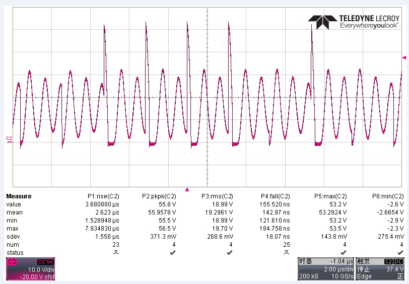
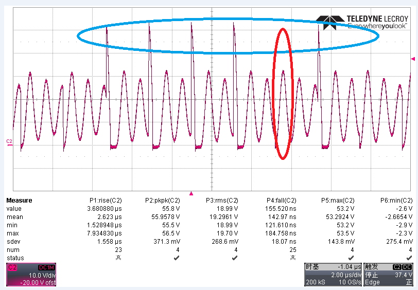
When the iout=0A, the LM5116 SW node waveform is as below. The LM5116 seems to be in diode emulation status. But it seems the LM5116 can't turn on the High side FET currently. When they increase the load, the LM5116 works in CCM normally. 

Is it normal? why?

  • Hello,

    Are you seeing the output as expected?

    This looks as expected. The high side FET will turn on for a short period of time, and then the ringing you see is due to both FETs turning off in order to increase the efficiency during no load operation.

    As you increase the load, then you will enter CCM operation.

    Best Regards,
    Katelyn
  • HI Katelyn,

    thanks for reply.

    The Vout is normal.

    The only problem is there is no high side MOS turn on interval in some cycles(the red circle). As i think, there should be Minimum HO on-time in every cycle, right? Thanks.

    Best regards

    Hollis

  • Hello,

    The high side FET turns on after the FB voltage falls below a certain level. Looking at what you have circled, this is DCM ringing, not a turn on of the high side FET. The five pulses that you have circled in blue look as though the high side FET is turning on. You can also compare this to the inductor current waveform to see when the inductor current is rising.

    Best Regards,
    Katelyn
  • Hollis ,
    Observe there are three unique states during each switching period in DCM operation. The first state is the ON state, when the High Side MOSFET switch is on and low side diode is off. The OFF state is when High Side MOSFET is off and low side diode is on. The IDLE state is during both MOSFET and low side diode are off. Ignoring the voltage drop on MOSFET and the diode, the voltage on Switch node node equals input voltage in ON state and equals zero in OFF state. The remainder of the switching cycle is the IDLE state when both MOSFET and diode are off. The current in the inductor is zero, and the voltageof the Switch node is expected to be equal to the output voltage. In reality, the switch node voltage waveform oscillates because the output inductor and the junction capacitance of the catch diode constitute aresonant LC network.

    As Katelyn pointed out , you can either observe the Inductor current or high side and Low side driver output to understand the operation better .

    Ambreesh