This thread has been locked.

If you have a related question, please click the "Ask a related question" button in the top right corner. The newly created question will be automatically linked to this question.

Regarding duty cycle operation above 50% on the OUTA/OUTB PWM outputs

Part Number: UC2825
Other Parts Discussed in Thread: UC3825, , UCC28950, UC3842, LM5045

Dear TI,

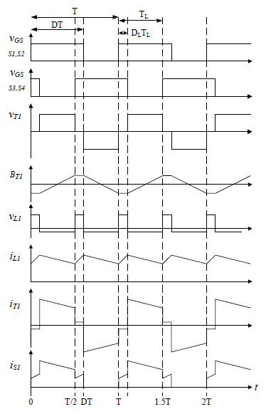
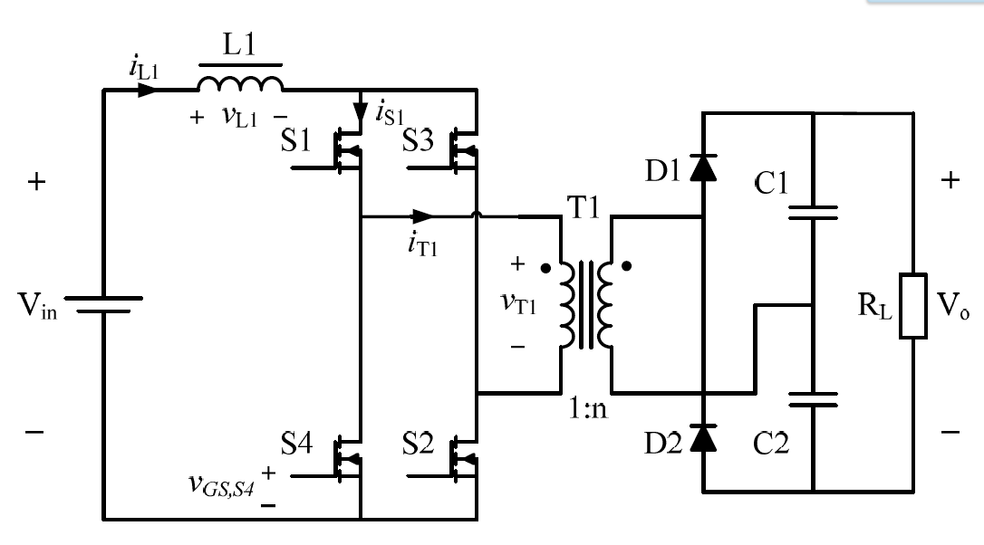
I have a question about the operation of the UC2825 IC for a Full Bridge Boost converter, with duty cycles above 50% on the alternating PWM outputs OUTA/OUTB. It is listed in the specs that the UC2825 can drive the two outputs up until 80% duty cycle (85% for the UC3825), but I have not found any evidence/applications of this in any of the datasheets/application notes. My application of the full bridge boost converter follows following switch, and component waveforms:

I am questioning whether the duty cycle could be expressed as a function of both of the outputs? Thereby limiting a duty cycle of 85% to be 85/2 for each leg of the H-bridge.

I need overlapping sequences of the complimentary H-bridge MOSFETs due to the Full Bridge Boost topology(see figure above), and it is therefore extremely important that I can have a duty cycle on each output above 50% for correct operation. I am looking for an IC that does this, as well as implements PCMC including slope compensation inputs.

If you can help me figure out if this IC can do this, or alternatively could point me towards any other IC that can do this, I would be most grateful.

Thank you for reading and helping me out! 
Best regards,

JC

  • Hello JC,

    I have not seen this topology before but believe there might an issue with it.  During the operation of this circuit most likely the current in iL1 will be a difference than IT1.  When this occurs the different the transformers primary current and the L1 current will have to go somewhere and will most likely cause over voltage stress on the FETs. 

    I would suggest a two stage approach instead.  For the boost converter you could use a UC3842 and for the full bridge you could use the UCC28950.  The UC28950 is a phase shifted full bridge converter that can achieve ZVS and there are many design tools available to help in the design process.  You can find information about the UCC28950 and design tools at the following link.

    Regards,

    Mike

  • Hello Mike.

    Thank you for your comments, but I am bound to use this hard switched topology and will stick with it for this project.
    I will have to use a clamp circuit to avoid over-voltage stress on the FET's. In the project I am using SiC switches to avoid high sw losses as well as an almost leakage free designed transformer.

    The topology uses two complimentary PWM signals 180 degrees out of phase, and the UCC28950 can not accomplish this, I believe.
    I know this is a rare topology and that is also why I would like to be sure about my request on the duty cycle of the IC.

    Do you instead happen to know of any IC that can generate two PWM signals 180 out of phase with duty cycles above 50%?

    Best regards,
    JC
  • Hello JC,

    I believe the LM5045 will meet your needs. The following link will get you
    to the data sheet. www.ti.com/.../lm5045.pdf

    Regards,

    Mike
  • Dear Mike,

    I am not sure if I am overlooking something in the component datasheet that you suggested, but from the section about the duty cycle feature, it is provided that the maximum duty cycle is below 50%. I have attached a figure with a snip from the section in the datasheet.

    Can you explain what I am missing here?

    Best regards,

    JC

  • Hello JC,

    I think that I see where your confusion is from.

    From the figure that you have have data sheet HO1 and LO2 are driven at the same time and HO2 and L01 are driven at the same time. When H01 and LO2 there is voltage being applied the transformer energy is being delivered to the secondary. When H02 and L01 are on at the same time energy is being deliver to the secondary. The effective maximum duty cycle is Tonmax/Tosc . However, they are choosing to evaluate the duty cycle of each energy delivery cycle separately. This would make the DC to DC transfer function of the voltage doubler as follows.

    Vout/Vin = D*Ns/Np +D*Ns/Np = 2*D*Np/Ns.


    Regards,

    Mike
  • Hi Mike.
    Thank you again for your fast responses!

    In that case I believe that I get exactly the same as the UC2825, where the outputs OUTA/OUTB are also driven individually up until 50% of the duty cycle, but with no assurance of how to use the dead-time intervals for proper overlapping due to a wanted duty cycle.

    The interesting part is the switching overlap, do you have any idea how I will generate this, based on the implementation of a PWM controller? It looks to me like dead-time between the switching cycles are the go-to in all the application/datasheets of PWM controllers. I struggle to find any documentation on how to ensure the on-time during the overlap phases of the converter.
    I hope you understand my concern, though there might be a straight-forward answer which I do not see...

    Best regards,
    JC
  • Hello JC,

    In a full bridge you want dead time between each gate drive to ensure you don't get shoot through. This is the FETs on the same side of the transformer on at the same time, which shorts the input to ground. This is why full bridge controllers are generally limited to 50% duty with some dead time.

    In a phase shifted full bridge you would adjust the dead time to achieve ZVS. The following application note explains how to accomplish this with the UCC28950. www.ti.com/.../slua560 . Please note I understand this is not what you are trying to accomplish. It is just to explain how you would generally setup the dead time for a full bridge with ZVS. In fixed frequency full bridge Dmax is generally 48% or less to prevent FETs on the same side of the HBridge being on at the same time preventing shorting out the input.

    The UCC2825 has two gate drivers operating at 180 degrees out of phase and are trailing edge modulated. If both gate drives are on at 60% they will overlap each other by 10%. In other words A and B would be on 10% of the period. If you increase this 75% you will have 25% over lap. If you have 80% you will both A and B on at the same time 30% of the time.

    You have a unique topology that I have not seen before and TI does not have application collateral or a control IC designed to support it directly. You may have to come up with something discreet circuitry to control the power stage.

    Regards,

    Mike