This thread has been locked.

If you have a related question, please click the "Ask a related question" button in the top right corner. The newly created question will be automatically linked to this question.

LMG1210: The datasheet talk about using a synchronous rectifier for the bootstrap diode. Which one and how to connect it?

Part Number: LMG1210

I have a technical question concerning the LMG1210.

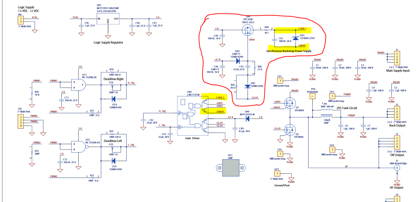
In the datasheet is written (section 9.2.2.2 Bootstrap Diode Selection): "For extrem cases, where the low-side FET on time is less than 20ns, TI recommends using small GaN FET as synchronous bootstrap instead of a diode. In this case, TI recommends ... to connect the source of the synchronous bootstrap directly to VDD."

I understand this section so, that I replace the diode with a GaN FET and connect the FET's source to VDD, the drain to the capacitor and the gate to the source. So I just use the FET's (very fast) body diode, right?

But when I do so (using GaN FETs from EPC), the maximum voltage for the high side switch is about 3.3V caused by the reverse drain-source characteristics of the body diode. Or am I understanding something wrong?

Do you maybe have a circuit as an example? Or a GaN FET with which you tested the bootstrap circuit of the LMG1210?

I want to use the LMG1210 with EPC's EPC2111 GaN half bridge.

  • Hi David,

    thanks for reaching out about this, let me make a SBD to show the connections and confirm with design the optimal solution and update you tomorrow asap.

    Thanks,

  • Hi David,

    below is a circuit of the sync bootstrap from EPC EVM board (epc-co.com/.../EPC9066_qsg.pdf)

    When the LO pin is HI, the gate of the sync bootstrap fet gets charged through R45.

    C45 pushes the gate to 5V above the 5V rail) When LO goes low, the gate is rapidly pulled back to 5V (0 VGS on the bootstrap device) through diode D45. So the bootstrap FET turns on when LO is on and turns off when LO is off

    There is a much faster charging of the bootstrap cap when the low-side is on because it is charged through a turned-on FET instead of through a diode.

    There is also no Qrr since GAN have no minority carriers involved in "diode" reverse conduction.

    This is the optimal solution as referenced from the DS. Let me know if you have any questions!

    Thanks,

  • Thank you very much. This answer helped a lot.

    Best regards,
    Arne