A related question is a question created from another question. When the related question is created, it will be automatically linked to the original question.
If you have a related question, please click the "Ask a related question" button in the top right corner. The newly created question will be automatically linked to this question.
Thank you for your interest in the UCC28780 ACF controller.
To start the IC, the SWS input (which feeds the VDD pin internally at start-up) must rise to 17.5Vdc. This means that the source pin of the depletion-mode MOSFET must also reach 17.5V. 25V and higher on the Depl-FET drain should be able to start it.
If you measure only ~3V on the Depl-FET source, then something is holding down the voltage, maybe by diverting the start-up current away from the IC.
Only a few milliamps are needed to charge up the VDD capacitors (through SWS input). Please check the components on the SWS pin and on the VDD pin to see if any of them are loading down the nodes when the voltage rises to about ~3V.
For example, if you have some comparators or op-amps connected to VDD, they may draw sufficient current at 3V to prevent further charge up of the VDD caps.
If no extra components are connected, check the parts that are there to make sure they are not damaged and leaking (such as a cracked ceramic capacitor).
Does this help? If not, can you provide a schematic diagram (can be partial) of the UCC28780 controller portion of your system?
I am not exactly sure... the datasheet of the BSS126 Depl-FET that we use specifies an on-resistance of ~320ohm for 0Vgs.
This is low enough to get many 10s of mA through the FET. The UCC28780 has a current limiting resistance of 12K when VDD < 1V and this decreases to 1K when VDD > 1V. So if Vsw = 30V and Vsws = 3V, then 27V/1.320K = 20mA charging current.
This seems to be enough to charge up the UCC28780 and most driver IC's as well. But if the series impedance keeps VDD below 1V, the internal R = 12K, so 27V/12.320K = 2.2mA. If the driver bias current exceeds this level at ~1V, it might be enough drain on the VDD to keep it from rising above 1V to switch in the lower series resistance.
Thanks, Ulrich. I'm checking circuit. If I don't use zener diode on HVG and SWS pin, what happened? As VDD on is ~18V, if use 18V zener diode, if have chance the circuit can't start up at all? Thanks again!
The zener diodes on HVG and SWS are intended for protection against abnormal over-voltage situations, as might happen with transient line events. They are intended to protect the BSS126 and HVG and SWS pins from overstress.
You are correct to think that with an 18-V zener on SWS, there is a chance that the IC may not start up. This may happen when the turn-on threshold is near the higher end of the tolerance range and the zener diode begins to clamp below 17V. For debug purposes, it is okay to temporarily remove the zeners to verify if they are interfering with start-up.
Please note: the protection on SWS should not be a normal zener diode not even a normal TVS. It should be a low-capacitance TVS (junction capacitance ~3-4pF) so that it does not slow down the dv/dt of the signal at SWS during run-time. A normal zener or TVS has far too much capacitance and will degrade the proper detection of the turn-on threshold at SWS (~9V for Si, ~4V for GaN) and make the turn-on timing too late. That then leads to hard-switching (no ZVS) and excess loss.
As you mentioned, the 18-V rating is too close to the 17.5V turn-on threshold for VDD. Proper Vz values for the HVG zener and SWS TVS should be between 20V and 24V.
Thanks for your detailed reply, Ulrich. As my driver IC Vcc connect with UCC28780 Vdd, while the driver IC max. Vcc is 20V and UCC28780 Vdd on is ~18V, so the working voltage range is pretty narrow. :) Why this part's Vdd on is so high?
The UC28780 is designed for off-line AC to DC conversion control. Like most other off-line controllers, it is expected to be able to self-start when AC power is applied, without requiring an external source of bias power. So the off-line converter must generate its own bias power, as well as regulate the main output(s).
Deriving bias power continuously from the high voltage rectified bulk rail is very inefficient, so instead, an auxiliary winding provides the bias current at low voltage once the conversion is underway. But to start up, a very low current is used charge a VDD storage capacitor up to the turn-on threshold. The controller consumes a tiny current (a few uA) during the VDD charge-up phase, but then consumes many mA (for IC bias and for MOSFET gate drive) once switching begins.
The aux winding on the primary side of the transformer delivers the higher bias current at the IC bias voltage usually (but not necessarily) below the start-up threshold. However, this voltage only appears when the output voltage rises as the output capacitor(s) charge up. And it must be maintained above the controller's UVLO shut-down threshold (below which the IC cannot function).
This ramp up does not happen instantaneously, but may take several milliseconds, or tens of milliseconds to happen if there is a load on the output while it is trying to start up.
Now, if there was a low start threshold voltage close to the shutdown threshold, it would take an enormous VDD cap to store the charge needed to keep the IC functioning while the outputs ramp up and the aux winding voltage rises high enough above UVLO to sustain operation. To avoid requiring a huge capacitor, it is better to charge a smaller value up to a higher voltage. Once that voltage reaches the high start threshold, switching begins and the cap voltage begins to drop as power is being process to the output.
The VDD cap is sized such that the output voltage and consequently the Aux bias voltage rises high enough to keep the VDD above the UVLO level, before the cap voltage is depleted to the UVLO level. So a start threshold that is many volts higher than the UVLO shutdown threshold allows a much smaller cap to be used than if the start voltage were only ~1V above the shutdown threshold.
ICs that have a narrow start/stop range are usually intended for use in applications where a separate bias supply is already available before the main power conversion begins. Ironically, most often such a separate bias supply for the narrow-range IC is provided by an off-line controller with wide-range start-stop VDD, such as is being discussed in this post.
I hope this clarifies the reason for the 18-V start-up threshold on the UCC28780. It is unfortunate that the semiconductor process used for the gate-drive IC design imposes a relatively low limit on VDD that squeezes the range to accommodate both devices.
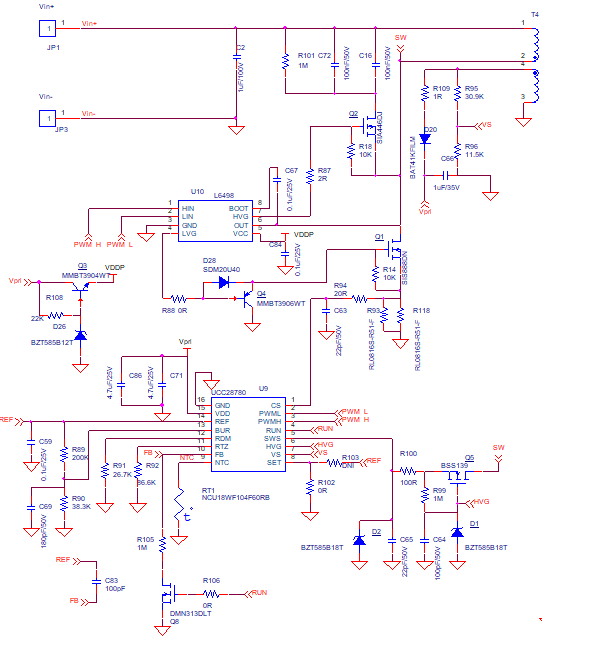
Appreciated your answer! Now I power up the board use two power source. One is for driver IC and the other is for Vin. But the board looks into hiccup mode.
Yellow is Vdd and blue is output of optocoupler. Can you see what's problem? Thanks.
I see the waveforms are operating in the "hiccup" mode, due to some unknown fault protection. Because several different faults at start-up result in the same symptom (VDD hiccup), the root cause of the shutdown must be diagnosed and corrected.
One clue might be the NTC input voltage. 47K should be a good resistance to start, but if you have any large capacitance on NTC, that can prevent start-up. Internally, the controller checks for NTC input voltage to be >2.2V at about 2us after REF rises to 5V. A large filter cap on NTC will delay this voltage rise and the IC may conclude that the ambient temperature is too hot.
To avoid any ambiguity, please remove any capacitance on NTC and remove the NTC resistor itself until after significant debug of your system is complete. NTC can remain open-circuit. That way the NTC fault will not interfere with debug operations.
I refer you to this start-up debug guide: www.ti.com/.../slua783.pdf
It is intended for primary-side regulators, but many of the start-up faults and remedies are the same as for the UCC28780.
Also, please refer to the UCC28780 datasheet and its tables of faults and descriptions of behavior for each.
Referring back to your original post, I realized that your input voltage range of 25~80V is not the normal "off-line" range that the design programs and the IC is optimized for. Therefore I first suspect that the start-up problem is related to the turn-on threshold setting for your design, although to may be something else. In any case, please follow the debug guide and use the fault behavior descriptions to figure out which fault is causing the hiccup shut-downs. You can use the rising edge of the optocoupler output as a trigger edge to capture the expected turn-on switching behavior that should be visible with a ~10us/div sweep on the scope.
I'll try to support your debug in a timely manner, but I am travelling this week and my responses may be delayed.
Good luck finding and correcting the problem and getting your design running.
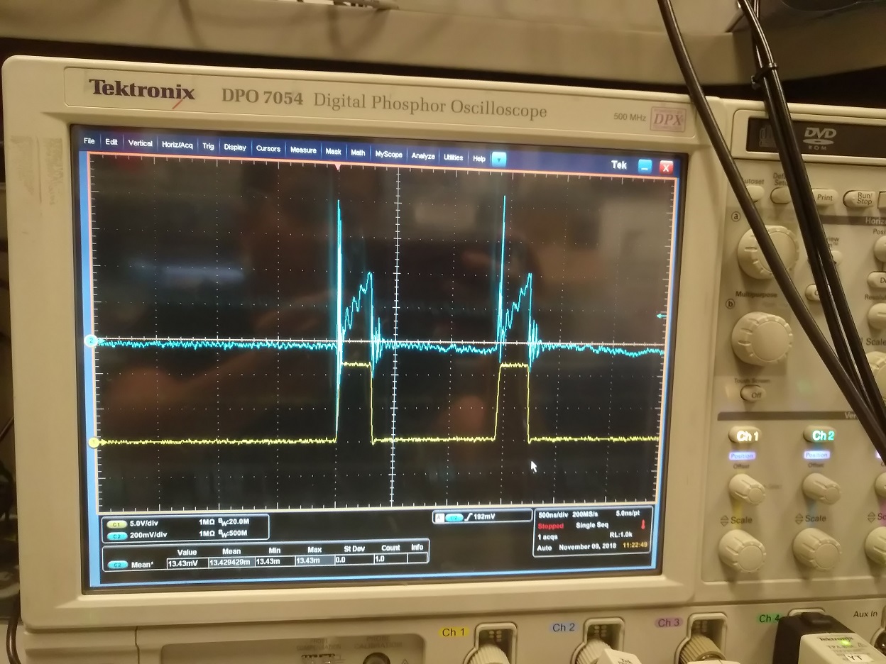
Today I test the PWML of driver IC and RUN signal. Attached waveform. When Vin is ~20V, there's one PWM, if increase to >30V, there's two PWM. Then hiccup.
I also attached my part of sch. Can you see any problems?
I am still travelling but I have a moment to address your questions which have accumulated. Starting with the schematic:
- My biggest concern is the capacitor on HVG, C64. It is shown as 100pF, but it should be 2~2.2nF. The HVG regulator needs it for stability to regulate the 11V on the Q5 gate. (This low cap value may have indirectly led to your earlier start-up issues.)
- My second concern is the 18V zener at D2, which should be a low-capacitance TVS (3~4pF) at 20~24V. A normal zener will add significant junction capacitance to the net and slow down the sensing of Vsw too much.
- Third is that the values for RDM and RTZ (R91 and R92 ) are calculated correctly. I can't check that because you do not provide any transformer information (Lm, Llk, Np, Ns, Na). You don't have to provide this, but please double check your calculations and use the most recent values for the equation factors. (Designers often change the values of various components during debug and forget to adjust other components whose proper values are dependent on the previously changed ones. Abnormal behavior may then occur.)
- Fourth is that the OPP adjustment resistor R94 is only 20 ohms. typical values are usually 50 to 100 times that, or more. However, I'm not sure what range it would be for a 30-80V input range. Still I think it would be higher than 20R. If the value is too low, then excess power can be delivered at high input voltage before OCP is triggered. If the value is too high then OCP kicks in too early at high line, and insufficient power is available.
Concerning the VDD hiccup:
The single PWML pulse at Vin = 20V is normal. This is a protection against an undetectable CS signal (if the input was shorted to GND, for instance). If the CS voltage does not rise to 0.28V within the time allowed by the SET setting (see datasheet page 35 on CS fault), the IC will conclude that CS is shorted and stop switching immediately after that first pulse. Your Vin = 20V is a condition such that the primary current cannot rise fast enough to meet this start-up criteria.
When Vin is higher at ~30V, CS-shorted fault is no longer detected, so more pulses are allowed. The should be at least three pulses (with hiccupping) after that until Vin is raised to the start-up threshold programmed by R95.
I don't know why you are getting only two. This seems abnormal, unless VDD is falling very quickly as these pulses occur so that UVLO is reached before the third pulse can happen.
Concerning the current peak (CS voltage) at 0.4V despite Vbur programmed at 0.2V:
This s most likely due to the driver propagation delay. If you display both PWML and LVG you can see the delay, which allows Ipk to go higher, even when PWML has gone low. The proper value of R94 (Ropp) will help mitigate the effect of this delay (and any others) for better Ipk control.
Using SET = 0V for a silicon MOSFET power stage may cause some subtle trouble, since the timing parameters for switching are affected. GaN FETs react much more quickly and have very low Coss, so the timing with SET = 0 is appropriate. High voltage Si-FETs are slower and SET = 5V provides better timing control.
However in your application, the 150-V FETs also have relatively low Coss, so the timing is relatively close that that for GaNs. It is hard to say if there will be significant trouble, but you may get better performance with one or the other. You may want to try both setting and compare. Refer to page 20 for details on the parameters that SET adjusts.
Leading-edge blanking time may be the parameter that gives you the most trouble, if it is too short.
I’m sorry for my delayed reply. I’ve been trying to catch up on work that has piled up during my travels.
I’ll try to address your questions and issues in the order of postings since the last time that I replied.
For your Nov 11 post:
It didn’t sink in (into my head), at first, that your input range of 20~80Vdc is unusual for this kind of controller. It is optimized for off-line operation (85~264Vac), and there are some de-optimizations that arise from the very low voltage range. I’ll address these as they come up.
Using Lm = 6uH results in a very high switching frequency for Si MOSFETs, particularly at high-line and light load. It could exceed 1MHz and the gate driver has too much delay time to be able to “keep up”.
I suggest to increase Lm significantly, such as 12uH or 15uH. This will require a redesign of the transformer, not just a simple reduction of gap width. How did you arrive at 6uH?
Also, a 10-W application is relatively low power for this kind of controller. Most applications range from 27 W to 65W, and some at higher power. Yours is the lowest Pout that I have come across so far, given the complexity of this topology. That is not to say that it can’t be done; just that it is unusual
For your Nov 12 post:
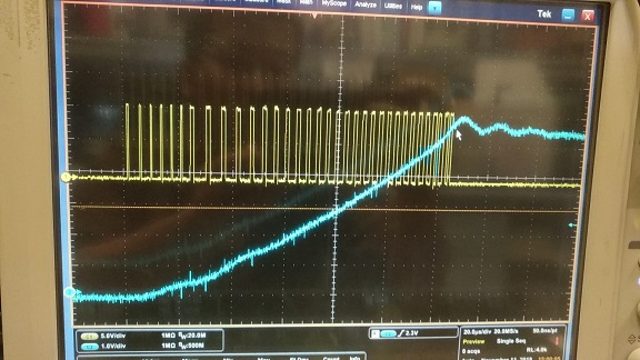
Vout is rising up but continues to rise past 5V without “slowing down”. This points to a feedback loop problem. The cause of the shutdown is not yet known. Originally I suspected OVP shutdown (as you do), but your next post has evidence against that conclusion. The rising ramp up through 5V suggests an open-loop condition. Or some incorrect value around the shunt regulator circuit. This part is not shown in your schematic segment of Nov 8.
For your Nov 13 post:
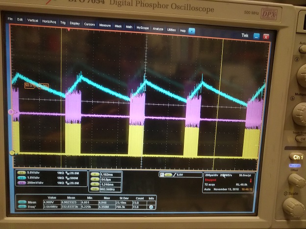
This behavior is abnormal output ripple, due to a large-signal problem, not a small-signal instability.
It resembles an OVP shutdown after each set of pulses, however it is not OVP because OVP would result in a shutdown interval of ~1.5 seconds.
I suggest to look at VDD on the UCC28780 controller and see if it is following a similar pattern. If it is, then the auxiliary winding is not keeping the VDD bias voltage up as it is expected to do.
The 12-V Zener D26 may be too low to keep the VDD voltage high enough after the Q3 base-emitter drop. Try a 13-V or 14-V Zener instead. (Or add a diode or two in series with D26 for a temporary test.)
For your second Nov 13th post:
It is possible that the CZRU52C20 zener diode is acceptable. I am not familiar with its specifications, but if the junction capacitance is low enough, it will not slow down the SWS signal significantly.
For your Nov 16 post:
Unfortunately burst-mode cannot be disabled. However, the excess “ripple” that you are seeing is not due to burst mode. It is from some kind of large-signal instability that we have not debugged yet.
This is not the normal behavior of burst-mode.
Can you please an up-to-date schematic diagram of the full power stage? If you wish to keep it private, please email it to ulrich_goerke@ti.com. This will help me to assess the entire power stage circuitry for anything not right. Meanwhile I suggest that you verify that each component on your board is the correct value and that all connections are solid. Often, the schematic looks good but the board has the wrong part, a backward part, or a bad connection that causes malfunctioning. One recent case had a Tl431 shunt regulator misconnected because the pinning of the actual device did not match the footprint on the board, but the schematic looked okay. It pays to double check.