This thread has been locked.

If you have a related question, please click the "Ask a related question" button in the top right corner. The newly created question will be automatically linked to this question.

TPS63070: Similar part recommendation and datasheet spec explanation

Part Number: TPS63070
Other Parts Discussed in Thread: LM5175,

Hi team,

The input range is 4.5V~12V, Vout is 5V, output loading is 3A.

I checked the website but seems we only support up to 2A solution which with internal FET, higher than 2A output current seems need to use controller.

I promoted LM5175 to customer but I would like to double check with you if there any other solution can meet customer's requirement.

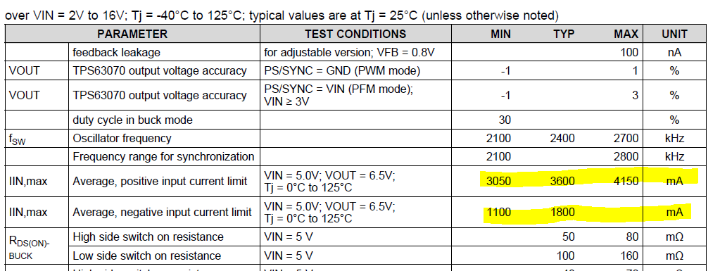
One more question about TPS63070.

What does positive and negative input current limit mean?

Are they specifying for different internal FETs? 

Are they specifying for average current of inductor?

Thank you.

  • Hi Wei-Ting,

    Unfortunately, we do not have a device for such current range. It might be possible to connect two TPS63070 in parallel to increase the current capability, but this is not completely tested.

    You might consider a 3 A buck converter with integrated switch, if losing regulation for the lowest input voltage range (<5 V) is allowed. In that situation buck converter would just feed through the input voltage.

    The current limits that you referred to are valid for the input pin. When operating in PWM mode, the TPS63070 is capable of sinking (negative) current on the output, although with reduced rating when compared to the sourcing (positive) current.

    Best regards,
    Milos

  • Hi Milos,

    3600mA is only specify for the FET which connect between VIN and L1? If yes, how about other FETs? or just limit one FET current, others will not be higher, right?

    3600mA is "average" of the triangular current waveform?

    Thank you.

    Regards,
    Wei-Ting
  • Hi Wei-Ting,

    Actually that is the current limit for both high side switches. Note that in boost mode the high-side buck switch (the one between Vin and L1) will have the highest current, and in buck mode the high-side boost switch (the one between L2 and Vout) will have the highest current. The current is measured on the high-side buck switch, but is also estimated for other switches, depending on the mode of operation. Whenever the limit is reached in either of the switches, the current limit kicks in.

    I think that should be clarified in the next revision of the datasheet.

    The current that is measured is the averaged current of the high-side buck switch. In boost mode this current is the same as the inductor current. In buck mode the current is measured while the high-side switch conducts, and for the rest of the period is reconstructed from the maximum inductor current and input/output voltages to obtain triangular current that corresponds to the inductor current.

    Best regards,
    Milos
  • Hi Wei-Ting,

    We haven’t heard back so we're assuming this answers your question. If not, just post a reply below, or create a new thread if the thread has locked due to time-out.

    Thanks,
    Milos