This thread has been locked.

If you have a related question, please click the "Ask a related question" button in the top right corner. The newly created question will be automatically linked to this question.

LM2623: LM2623 Problem with AP22802

Part Number: LM2623
Other Parts Discussed in Thread: TPS61256

Hi Team.

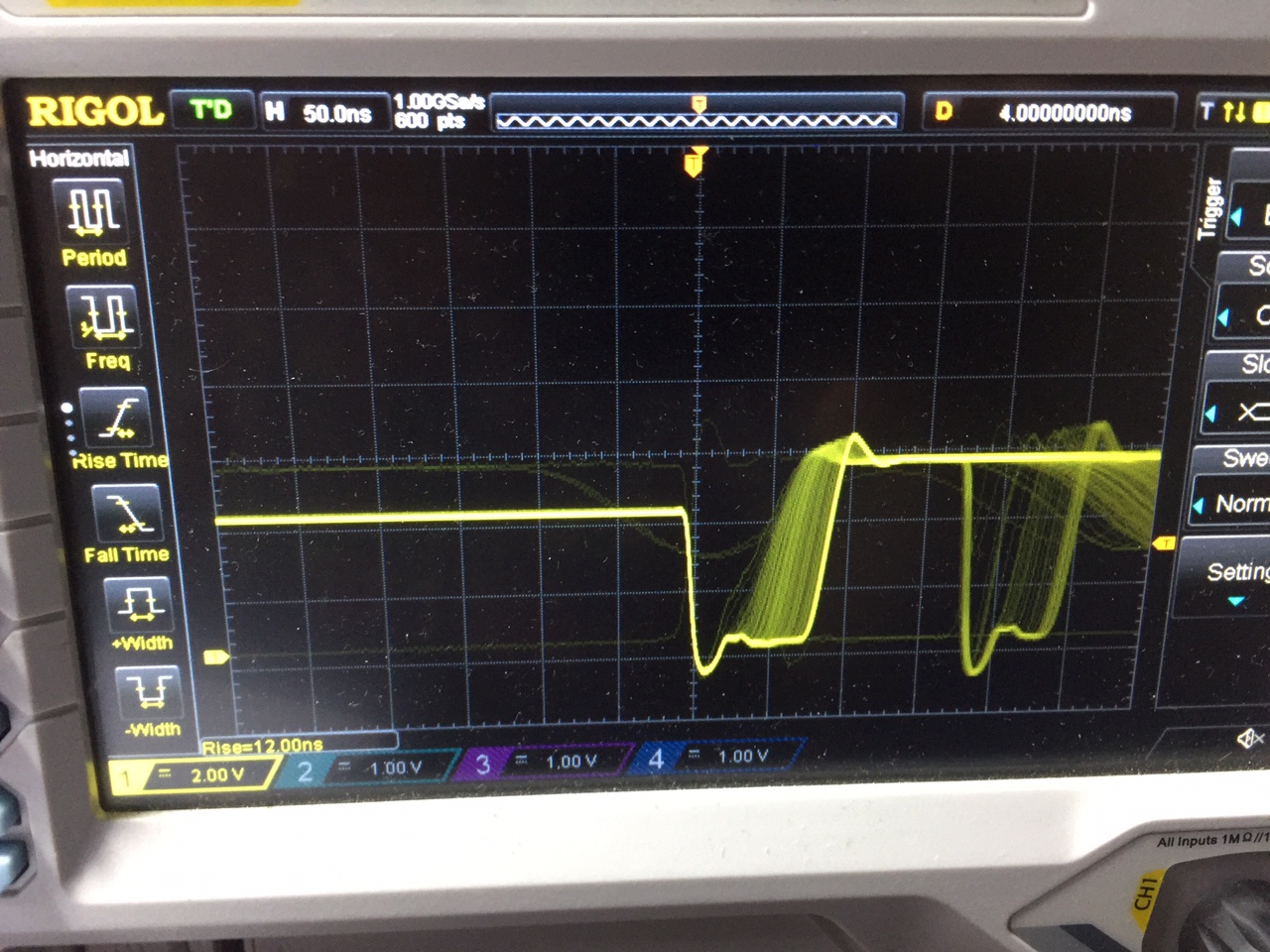
I have just design PBC using LM2623(schematich design as picture below), but it is not working now and i can not find the reason.

I have checked on PCB

1.VOUT_BQ = 4.1V

2.When i enable  EN_5V_SW = 3.3V then U18(AP22802AW5-7) is warmup and U17 have not Vout, this mean VCC_5V_SW about 0V

Any one can find and give me solution about this problem

I’d greatly appreciate your Support

  • Hi Hoang,

    Have you checked the voltage of U18 ouput and SW pin voltage? Because if everything is correctly soldered and not broken, SW pin voltage should be the same with U18 output voltage. VCC_5V_SW will be a litthle lower than U18 output voltage.
  • Hi Zack Liu..

    Thanks you for your response.

    I have checked as bellow:

    1. When i take out R86 and L13 on the PCB. voltage of U18 ouput = 4.1 V

    2. After that i assembly and solder R86 and L13 agian..I checked Voltage in Anode D7, it is about 0

    Could you give me the solution for my problem.

    Thanks you very much.

  • Hi Hoang,

    From your description, the AP22802AW5 is working properly. How much is the load current of LM2623?
    Could you also just supply LM2623 directly using an power supply to see whether the boost converter is working correctly.
    If possible, you can also share the PCB layout.
  • Hi Zack Liu.

    Thank you for your respone.

    1. The load current of LM2623, it is about 70-100mA

    2.When i supply LM2623 directly using a power supply, it is working correctly

    I'm afraid that, When LM2623 have out put voltage about 5V that mean Vout AP22082AW5 about same 5V and it is bigger than Vin AP22082AW5 (4.1V).

    Do you have other IC load switch from TI, that can run smoothly when Vout > Vin ?

    I have atached PCB as bellow, please help me find the reason and solve that problem

    One again, thanks you very much.

    LM2623.pdf

  • Hi Hoang,

    What do you mean "When LM2623 have out put voltage about 5V that mean Vout AP22082AW5 about same 5V and it is bigger than Vin AP22082AW5 (4.1V)."?
    If the both the load switch and boost converter can work properly, could you use probe to measure some key waveform?
    1. When EN_5V_SW is on, see U18 output voltage, U17 sw pin waveform.
    2. Use current probe to monitor the input rush current at the input of U18 to see if it is the reason of rush current that cause the load switch to shut down.
  • Hi Zack Liu.

    I Have used probe to measure probe form anode and cathode of diode D7 (with out use AP2208, because when i add AP2208, it is not have wave form, about 0V) waveform as below picture:

    What do you mean "When LM2623 have out put voltage about 5V that mean Vout AP22082AW5 about same 5V and it is bigger than Vin AP22082AW5 (4.1V)."?

    my mean is: pin 1(OUT) of  AP22802 is conneted directly with pin 12 and 13(SW_12, SW_13) of LM2623. So when Pin SW_12 and SW_13 go to minus -> Pin OUT's AP22802 i minus.

    I think this is root cause of my proble i have.

    Could you give me solution for my proble.

    Thanks and best regards!

  • Hi Hoang,

    "pin 1(OUT) of AP22802 is conneted directly with pin 12 and 13(SW_12, SW_13) of LM2623. So when Pin SW_12 and SW_13 go to minus -> Pin OUT's AP22802 i minus."
    There are still inductor between Pin 1 of AP22802 and Pin12,13 of LM2623. When LM2623 mosfet turns on, SW pin voltage goes to zero, the voltage across inductor L13 is Vin, then current of inductor goes high. When LM2623 mosfet turns off, SW pin voltage equals Vo+Vdiode, the volatge across inductor L13 is Vin-Vo=Vdiode, which is minus, then inductor goes low.

    Now it seems the LM2623 boost converter is working correctly. It seems there is some problems with load switch AP22802. What's the maximum current that AP22802 can hold? Now the total output capacitance is over 200uF, and it will cause a big inrush current when the Vo rises. You could try use a smaller Co or try startup with no load.
  • Hi Zack Liu.

    Thanks you for your respone.

    I have checked datasheet's AP22802 and found that:

    In my design Vin Ap2208 is connect directly to Vout_BQ(It is about 4.2V)...When LM2623 boost to 5V. that mean Vout AP2208 is about 5V.

    But in datasheet AP2208 Vout form -0.3 to Vin+0.3. (actual Vin = 4.2V, Vout =5V).

    I think this is root cause and when AP22802 connect with LM2623 then they cannot run normal. But when they run separate they run normaly.

    Could you give me the solution for my sittuation.

    Thanks and Best Regards!

  • Hi Hoang,

    I think you misunderstand how the LM2623 works. LM2623 is a boost converter that output voltage is higher than input voltage. If the whole circuits works properly, the input voltage of AP2208 will be 4.2V, Vout of AP2208 is 4.2V(may be 4.1V). Vout of LM2623 is 5V. The SW pin of LM2623 is 0 or 5V.

    What's the FLG pin voltage when Vout of AP2208 is 0? You could power up the whole system without connecting load resistor first.
  • Hi Zack Liu
    I'm sorry about late my respone
    I have checked system without connecting load resistor as your suggest.
    1.the FLG pin voltage is 0 when Vout of AP2208 is 0 (enable AP2208)
    2.the FLG pin voltage is 4.2V when i disenable AP2208.
    could you give me next step to solve my proble
    Thanks and Best Regards!

  • Hi Hoang,

    For AP2208, Open-Drain flag is active low when triggered. It should be triggered because of overcurrent. I think you misunderstand my meaning. I mean when AP2208 and Lm2623 is both connected well and AP2208 EN pin is logic high, what's the FLG pin voltage.
    Before asking you to do more tests, I'd to confirm some thing with you:
    1. What's the value of the load resistr? When you didn't connect load resistor and enable load switch AP2208, is the LM2623 Vo correct?

    What I hope you can test is:
    1. Could you solder a current lope in series with the inductor L13? Take a picture of the startup inrush current when the circuits is powered up and AP2208 is enabled.
    2. Do you have any other higher current level load switch? If you have one, please change it with new one.
  • Hi Zack Liu.

    I have checked when AP2208 and Lm2623 is both connected well without Load, result as bellow:

    1. The FLG pin voltage is 0V when Vout AP2208 is 0V, Vo LM2623 is 0V (Enable AP2208 PIN EN =1)

    2. The FLG pin voltage is 4.2V when Disable AP2208 (PIN EN =0)

    About your require.

    1. Due to my PCB is very small so i can't  solder a current lope in series with the inductor L13. But i can solder resistor parallel with inductor L13. Do you have other way for this case?

    2. Currenly i don't have any other higher current level load switch. But i will order other Load Switch AP22814AW5-7 with 3A current from digikey and test it.

    During i'm waiting other load switch to replace. Do you have any suggest to detect my issue for nex step?

    Thanks Anh Best Regards!

  • Hi Hoang,

    Thanks for providing these information. Now it seems the boost converter is working correctly if without the load switch. I recommend you choose a higher current value load switch and then test it again.
    Do you really need the load swtich? Because LM2623 itself has an EN feature that you could it to enable/disable the converter.

    You can solder one side of the inductor on the pcb. Make the inductor vertical with pcb so that a wire could be soldered in series with the inductor.
  • Hi Zack Liu.
    Thanks you for your response.
    First time I have idea same your suggest, that is use pin EN of LM2623 to control ON/OFF boost VCC_5V_SW.
    But I think VCC_5V_SW will have power when I disable pin EN of LM2623 due to power supply will pass via diode D7 to VCC_5V_SW, that is right?
    Do you recommend to me the value of resistor when I solder series with the inductor L13 to make measure current when power startup?
    As last your replay "Now the total output capacitance is over 200uF", could you let me know how do you calculate value 200uF?

    Thanks and Best Regards!
  • Hi Zack Liu!

    I give to you more information about my design

    1. About VOUT_BQ, it is pin VOUT(pin 10,  11) of  BQ24072RGTR

    2. When power startup, we have 2 boots power operate at the same time.

    I hope this information will help you find solution for my issue.

    Thanks And Best Regards!

  • Hi Hoang,

    1. Yes, even though you disable EN pin of LM2623, there will still a voltage (Vin-Vdiode) on the output of LM2623.
    2. Just solder a wire in series with inductor to see the current wavefrom if you have a current probe. If you don't have one, use a 100mohm resistor in series with the inductor.
    3. When powers up and VCC_5V_SW drops down to 0, how about the voltage of Vout_BQ, VCC_3V?
  • Hi Zack Liu!

    Thank you for your responses.
    1. When powers up and VCC_5V_SW drops down to 0, Vout_BQ, VCC_3V is run normally, that mean Vout_BQ =4.2V, VCC_3V = 3V3.
    2. Because when disable EN pin of LM2623, there will still a voltage (Vin-Vdiode) on the output of LM2623 so that I use AP2208 to control input power. Do you have any idea to control input power VCC_5V_SW without using AP2208? My purpose is ON or OFF VCC_5V_SW to reduce power when no need.

    Thanks and Best Regards!
  • Hi Hoang,

    TPS61256 has a wide Vin range from 2.3V to 5.5V and it has true load disconnect during shutdown feature. You could try it.
    If you still want to use LM2623, choose another load switch.
  • Hi Zack Liu!
    Thank you for your support during I have problem with LM2623.
    Maybe I will waiting until I have another load switch to continues testing.
    So could you suggest me IC have package same BQ24072RGTR, but it have Vin lower than BQ24072RGTR?
  • Hi Hoang,

    You could send a new post related to BQ24072RGTR, out colleagues of chargers will answer you. Thanks.