All the I/O in my design is 3.3V. I'm using the TPS65070 to power the '674x and an Altera FPGA. I hoped someone could tell me if I'm on the wrong track. Where I deviate from the reference design is in red.
DC-DC#1: 3.3V/600mA - I power the I/O and all other 3.3V off this. I believe 600mA is enough b/c I'm not going to I/O pins sourcing that much current.
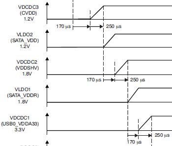
DC-DC #2: 1.8V/1.5A - I power DDR memory and anything else that is 1.8V from swticher #2 EXCEPT for USB and SATA power (required to be powered on Si prior to v2.0 even though we're not using it).
DC-DC #3: 1.2V/1.5A - DSP and FPGA cores. We will need most of the 1.5V, but it should be enough.
LDO#2: 1.2V/200mA - CVDD and RVDD only
LDO#1: 1.8V/200mA - USB and unused SATA power.
Questions:
- In the reference design (page 72 of the '65070 datasheet), LDO1 (1.8V/200mA) has a FET to delay this supply to prevent it from coming up until the I/O voltage is present. I cannot understand this b/c the TPS65070 default has the LDOs not starting until DC-DC #3 (1.2V) is up. The power sequencing requires 1.2V to come up before 1.8V, but it does not require 1.8V to come up after I/O. Moreover, DC-DC #2, which is typically used for I/O, and the LDOs both come up ater DC-DC #3 is stable. Can you explain the purpose of that FET?
- Is there anything bad about my plan of powering the memory controller and the DDR chip with DC-DC #2? Do I need to extra filtering? Some of the memory ICs we considered have instantaneous current draw of 200mA+, so I'm reluctant to use the LDO to power memory?