


Other Parts Discussed in Thread: BQ34Z100-G1
Hello there,
I have noticed a slight inconsistency between the reference designs of BQ34110 and BQ34Z100-G1. Here is the one for BQ34Z100-G1 (SLUSBZ5B –JANUARY 2015–REVISED JULY 2016):
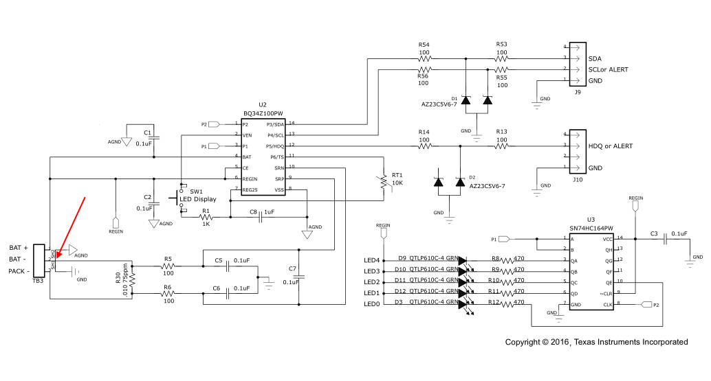
Notice where is the common ground for the U2 and U3 chips. Now the reference design for BQ34110 (SLUSCI1B –AUGUST 2016–REVISED NOVEMBER 2016):
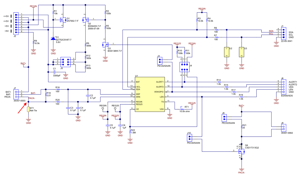
The common ground is referenced to PACK- line, not BAT- line, like for the BQ34Z100-G1.
Correct me if I am wrong but this is how I understand the difference:
- For the first schematics, the BQ34Z100-G1 is unable to measure the current that this circuit is drawing, since its bypassing the shunt resistor.
- The logical levels on the I2C line with the master devices will be offset by the voltage drop on the shunt resistor.
------------------
- For the second schematics, the device can measure the current that this circuit is drawing, since it doesn't bypass the shunt resistor.
- The logical levels for I2C between this slave and the master are correct.
If what I have written is correct, where does the difference in designs come from? Is there something else I don't see here?
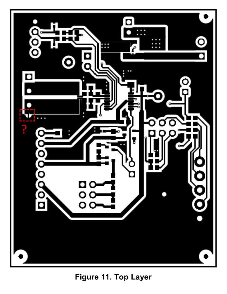
PS: What is NT1 (Net tie)? Is it just a way to trick Altium into connecting 2 different nets together without using an actual 0R resistor? How does this component look on the PCB? Is it this one?
I would appreciate all help.

