This thread has been locked.

If you have a related question, please click the "Ask a related question" button in the top right corner. The newly created question will be automatically linked to this question.

TPS2663: Clarifications

Part Number: TPS2663
Other Parts Discussed in Thread: CSD19537Q3

Hi All,

We are planning to use TPS26630 for 24VDC input.

Below are the clarifications,
 #1: When we use 2 no of TPS26630. Can we able to OR the input side and output side? Do we need to take care any additional protection for ORING?
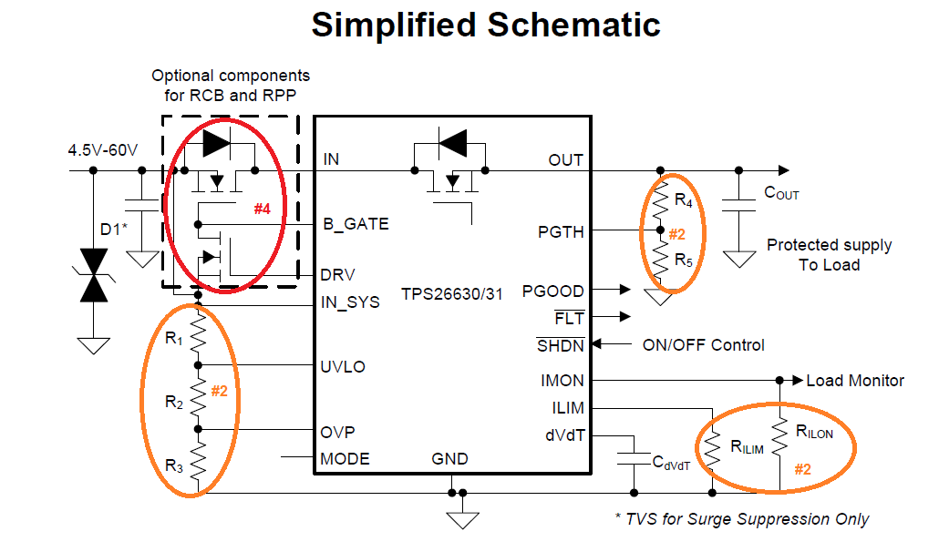
 #2: The operating voltage level will be 18V DC to 36V DC. What will be the resistor wattage level needs to be used?
 #3: As per the datasheet Page no:6, the maximum voltage level for shutdown pin will be 5V. Can we able to give 12V DC or 24V DC?
 #4: Is it mandatory to use, 2 no of FET's on input side(FET-1 to Pin 1,2,24, FET-2 to Pin 3,4)?
     As per the datasheet, it is mentioned FET components are optional.
 #5: In case if we are using FETs, Do we need to give the Pull up resistors before FET or after FET?

Regards,

S.Saravanakumar

 hat will be the

  • Hello Saravanakumar,

    Please find replies below:

    #1: When we use 2 no of TPS26630. Can we able to OR the input side and output side? Do we need to take care any additional protection for ORING?

    ORing can be implemented with TPS2663 devices. Section 10.3.2 on Page 27 of the datasheet illustrates priority power mux operation with ORing of two power supplies (MAIN & AUX). In this example, the load is powered either from VIN_MAIN OR from VIN_AUX.

    if both supplies (MAIN & AUX) are available, load will be powered from VIN_MAIN.

    #2 The operating voltage level will be 18V DC to 36V DC. What will be the resistor wattage level needs to be used?

    Resistors R1 to R3, R4,R5, RILON, RILIM are not in the power path and these can be of low wattage (< 0.25W).


    #3: As per the datasheet Page no:6, the maximum voltage level for shutdown pin will be 5V. Can we able to give 12V DC or 24V DC?

    The recommended operating condition (Table 8.3 in Datasheet) for SHDN pin is 0 to 4V.

     #4: Is it mandatory to use, 2 no of FET's on input side(FET-1 to Pin 1,2,24, FET-2 to Pin 3,4)?
         As per the datasheet, it is mentioned FET components are optional.

    FET-1 and FET-2 are optional FETs for Reverse current blocking (RCB) and Reverse polarity protection (RPP). FET-1 is a power FET (similar to CSD19537Q3) for Reverse current blocking (RCB) and Reverse polarity protection (RPP) while FET-2 is a signal FET (similar to BSS138) for quick turn-off of FET-1.

    #5: In case if we are using FETs, Do we need to give the Pull up resistors before FET or after FET?

    There are not external pull up resistors for FET-1 and FET-2. You can refer to typical application circuit (Figure 16 on Page 23) of the datasheet.