Other Parts Discussed in Thread: TPS54140, TPS54160, TPS54160A
I have a ripple problem with TPS54140A in very small load (<50mA).
The ripple wavefroms are (1) shown below.
So I selected a low inductance to reduce the ripple.
(2) is the circuit diagram, and (3) shows the waveforms(IL and Vout) captured from this circuit.
I wonder the circuit (2) is a correct solution for a very small load application.
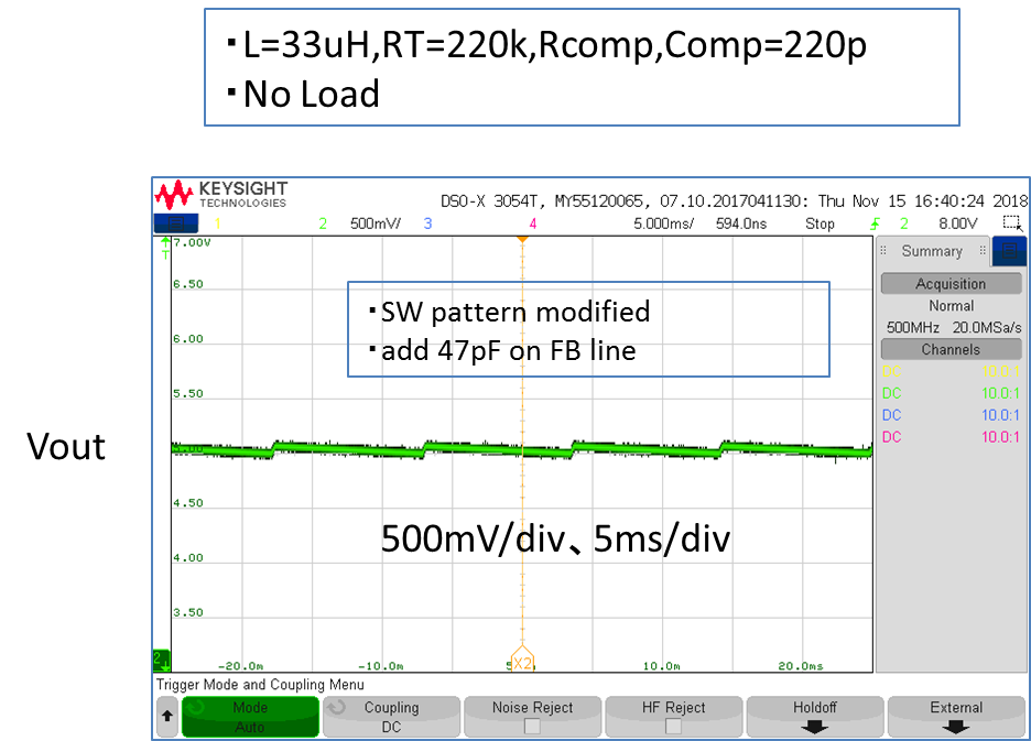
If there's a problem or an advice, Please let me know. It would be very helpful.
Regards,
(1) Comparison of different inductance value (when no load attached)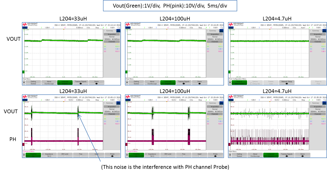
(2) Circuit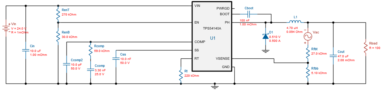
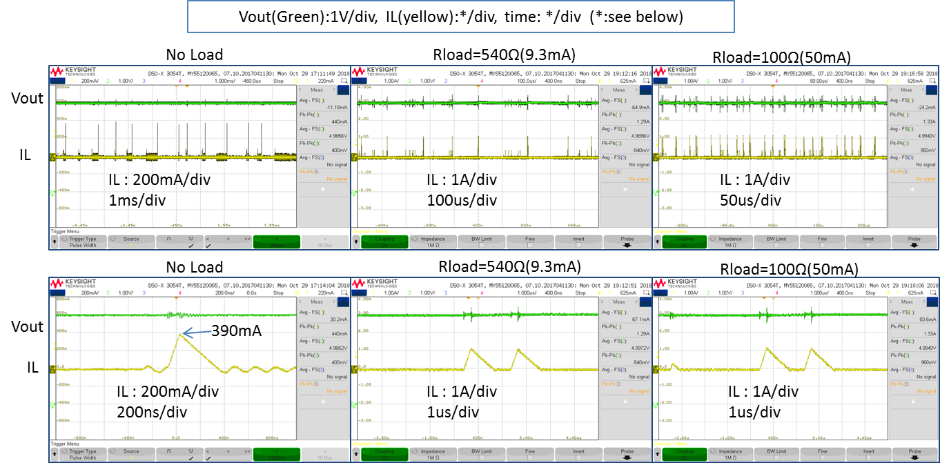
(3) Comparison of different Loads with inductance=4.7uH (above circuit diagram)