This thread has been locked.

If you have a related question, please click the "Ask a related question" button in the top right corner. The newly created question will be automatically linked to this question.

TPS54361: Irregular SW node at specific Vin

Part Number: TPS54361

Hello,

We are trying to troubleshoot this power supply:

  • Vin=12V to 36V
  • Vout=6.5V
  • Iout=.8A

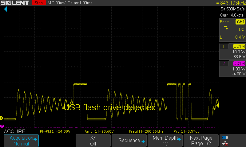
Issue: At 21V-23V input, there is irregular SW node waveform and audible ringing. Potentially an issue with compensation. These images were captured with 220pF in parallel with the series combo of 22nF and 20kOhm. We have tried others from the excel calculator without much success, but we will try other you recommend.

Can you suggest some tweaks to solve this? Thank you!

Image 1: Below 20Vin, SW node looks normal

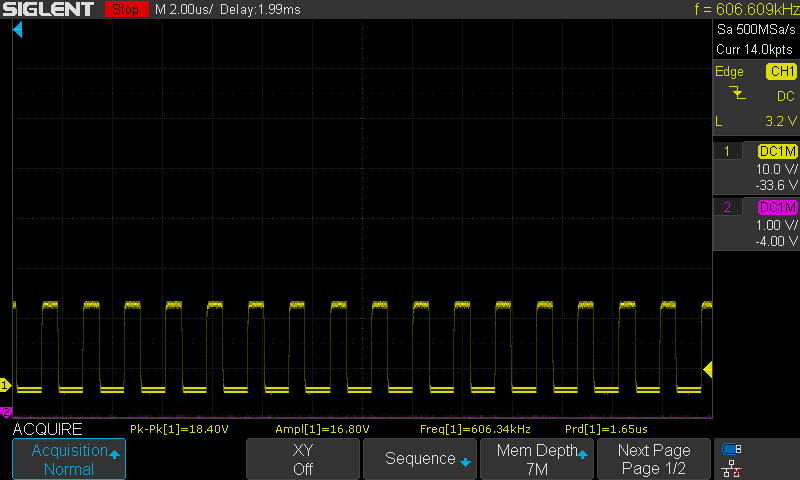
Image 2: At 21V to 23V input we see a choppy SW node. The sinusoidal ringing seems typical from pulse skip waveforms. Audible noise is present here.

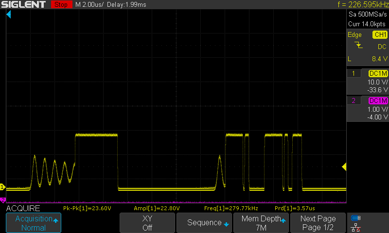
Image 3: Over 24V input the SW node looks good again

Image 4: Here is 23Vin but with the load removed, still minor oscillations but no audible noise.

  • Hi Ryan,

    Please send the schematic and layout.

    Regards,
    Tim
  • Hi Ryan,

    As Tim suggested, do you have schematic/layout of this design?
    Also when you at 24VIN, I can see that the frequency is different from what you have at below 20VIN, eventhough the switch node looks like normal.

    Thanks
    -Arief
  • Hi Tim, Arief,

    Thanks for the quick response. Schematic sent offline, layout to follow.

    Is it possible for poor compensation to cause such a dramatic frequency shift?

    It is worth noting that an earlier revision of the board did not have this problem, so perhaps layout is at fault even though I'm told it was only slightly tweaked from old board to new board.

    Regards,
    Ryan B.

  • Hi Team,

    Layout has been sent.

    Also wanted to note that the device is still regulating the 6.5Vout, albeit with some noise around the problem areas.

    Any ideas on the compensation and/or layout are appreciated!

    Thanks,
    Ryan B.
  • Hi Tim, Arief,

    To close this thread and leave tips for whoever may find this post:

    -The first concern was that the FB trace was too long and too close to the switch node. We tried lowering the FB resistor values by 10x to increase noise immunity, but this brought no improvement.

    -What worked was placing a 100pF capacitor in parallel with the frequency setting resistor. This partially makes sense since we were seeing such huge swings in frequency. The frequency resistor did not seem to be in a noisy spot on the board, but for now this issue is resolved.

    Thanks again,
    Ryan B.