Team,
Customer is testing TPS2546 in notebook system and got below waveforms.
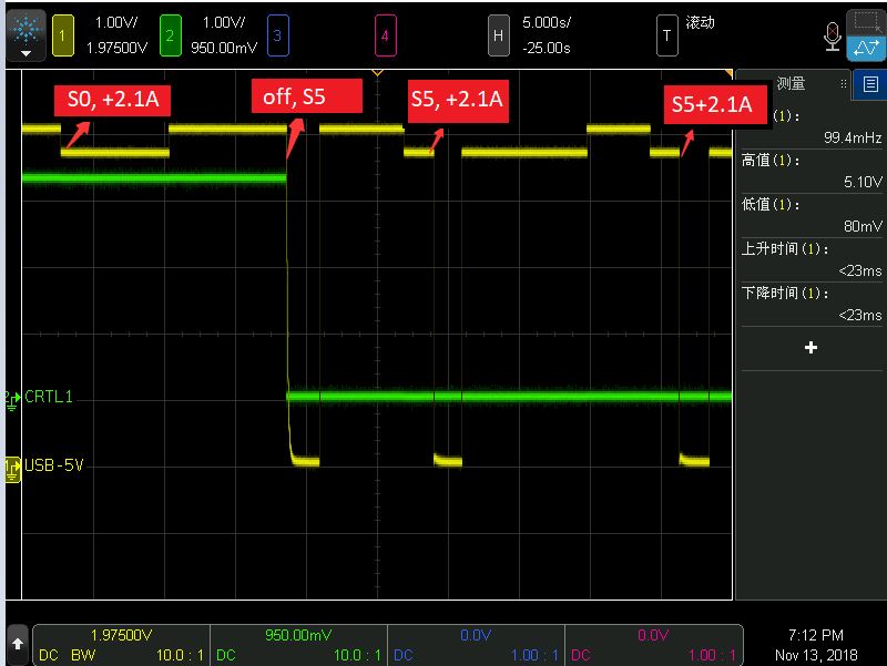
1. When system in S0, CTRL1/2/3=111; When system in S5, CTRL1/2/3=011.
2. When system in S0, drive current 2.1A,there is no VBUS drop.
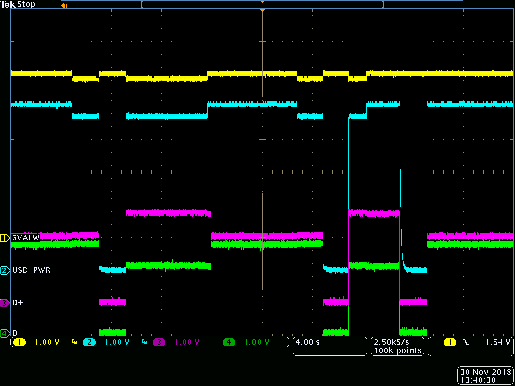
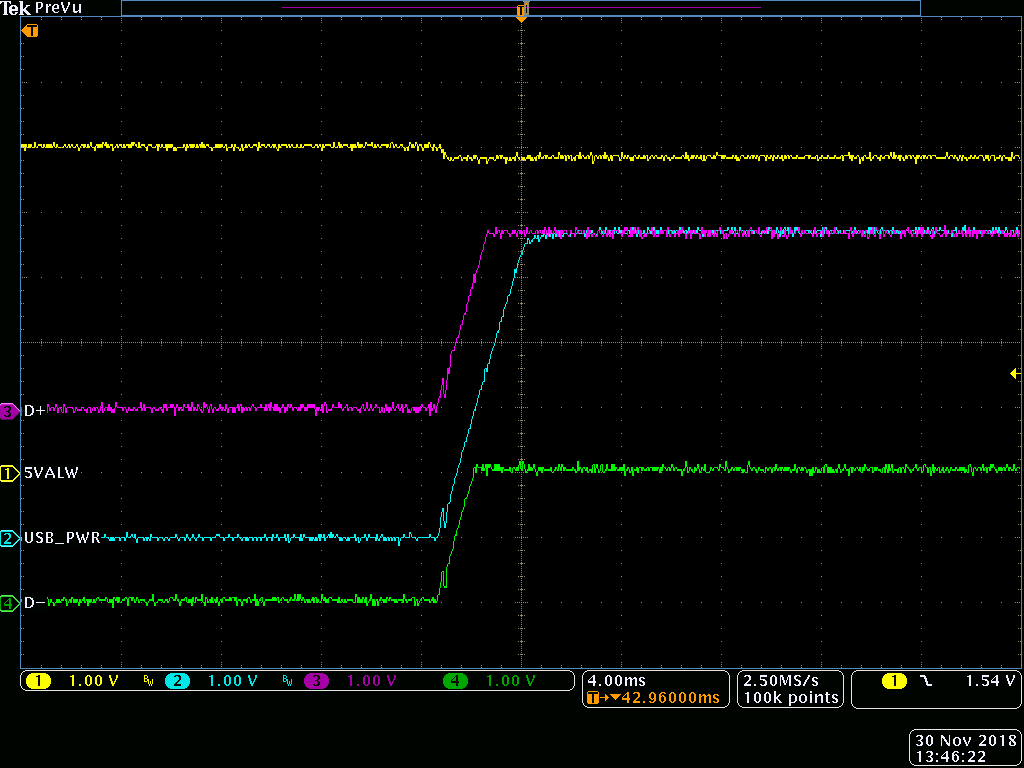
3. When system shut down, change from S0 to S5, CTRL1 change from 1 to 0, VBUS will drop to 0 and then back to 5V, is it normal?
4. When system in S5, drive current 2.1A, VBUS will drop to 0 and then back to 5V as well, is it normal?
Could you let me know where I can find the explanation in datasheet? Thanks.
Note: in below waveform, 抽载means drive current 2.1A, 关机means system shut down (change to S5)