Hi Team
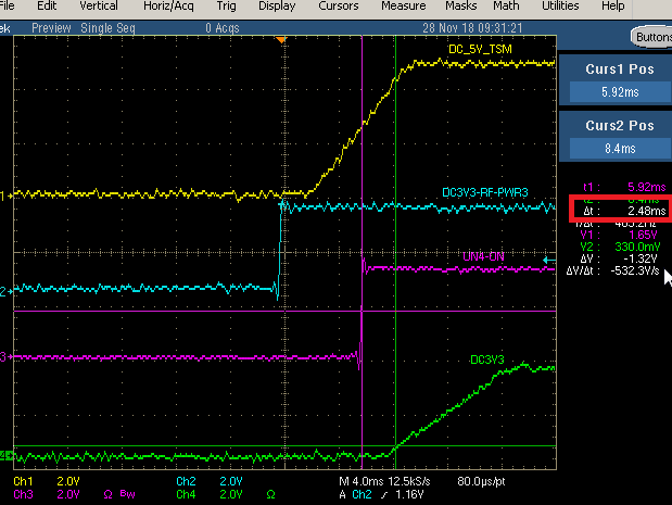
I want adjustable rise time. TPS22975 Datasheet P.15 Vout rising time formula is Vbias =5V.
SR = 0.43 * Ct + 26
But my Vbias = 3.3V.
How did I calculate the slew rate ? same Calculation formula ?
Hi Team
I want adjustable rise time. TPS22975 Datasheet P.15 Vout rising time formula is Vbias =5V.
SR = 0.43 * Ct + 26
But my Vbias = 3.3V.
How did I calculate the slew rate ? same Calculation formula ?