This thread has been locked.

If you have a related question, please click the "Ask a related question" button in the top right corner. The newly created question will be automatically linked to this question.

TPS5430: TPS5430 radiated EMI

Part Number: TPS5430

Hello,

I use your TPS5430 DC/DC converter in my products. I went to certification house to measure radiated EMI. The results were bad, and there were large spikes above 40 dBuV(limit according to CISPR22). In the end, I found that the problem is in DC-DC converter because after connecting external 5V supply, the problem disappears and the results were fine.

How is this possible? I made layout according to your specification. Is there any way to solve radiated EMI?

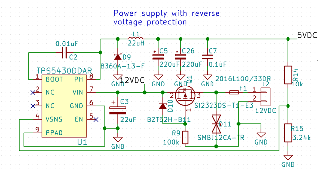
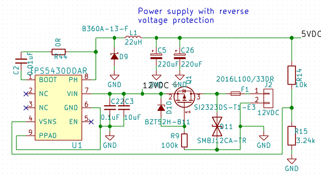
Here is my schematic.


Kind regards

  • Hi Ninoslav,

    Please forward your layout for review. Also, you can read this article series on EMI (part 4 in particular is on radiated emissions).
    www.how2power.com/.../EMI_Guide.php

    Regards,
    Tim
  • Hello Timothy,

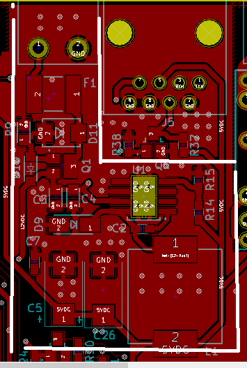
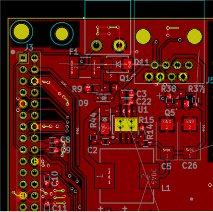
    Thank you for your answer. Here is my layout (I showed just top plane). Maybe something is not according to layout example from TPS5430 datasheet, but I don't think this can produce such differences in radiated EMI measurements.  Maybe some external or additional component should be added?  Please give me some suggestion.

    Kind regards,

    Ninoslav

  • Hi,

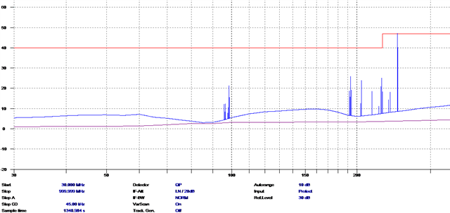
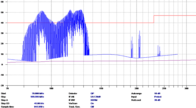
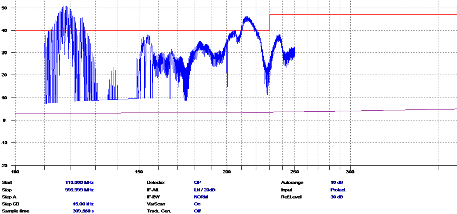
    Here are our measurements:The first picture shows radiated emissions using external 5V power supply.  The second picture shows radiated emission when TPS5430 is running.

    Kind regards

  • Hi Ninoslav,

    Here are some options:

    (1) Try adding a small resistor (e.g. 10 Ohms) in series with the boot cap to reduce the turn-on speed of the high-side MOSFET. This reduces the dv/dt of the SW node voltage. Alternatively, you can add an RC snubber from SW to GND to achieve a similar effect.

    (2) Reduce the loop area of the high-side MOSFET, freewheeling power diode and input capacitor as this loop has high di/dt. Place a full GND plane on layer 2 immediately below the power stage components on layer 1 and use a low interlayer spacing (e.g. 6 mils).

    (3) Use a shielded inductor to curtail emissions from the inductor.

    Regards,
    Tim
  • Hi Tim,

    Thank you for your answer. I am not sure if adding either boot resistor or RC snubber will solve the problem. This is our 4th. revision and I am scared if your proposals aren't an exact solution (because your 1st. option isn't in datasheet even). I have the full ground plane on the bottom layer just below this components, and loops aren't so huge to cause such EMI.

    Perhaps, some less noisy DC/DC converter is the solution?

    I tried to add PI LC filter on the input to prevent emission, results were even worse (please look in the picture). Two phenomena can be possible to describe such behavior:

    1) Inductor as a part of PI filter is unshielded one and that is the cause of emissions.

    2) Inductor connected in series with the drain of high power MOSFET creates destructive back EMF when MOSFET is switched off (that happens every 1/500 000 for this DC/DC converter).

    Any advice is welcome.

    Kind regards

  • Hi Ninoslav,

    It's a good idea to only use shielded inductors, both for the buck inductor and the input filter choke.

    Looks like you're failing in the 85-130MHz region. This typically corresponds to the switching waveform rise and fall times. To reduce dv/dt and spike overshoot of the rising SW node voltage, an easy test is to connect 10 Ohm in series with the boot cap. Please send the SW node voltage waverform for review (measured with probe tip and barrel approach - ground lead removed).

    Another important point is to connect a 10-100nF input ceramic capacitor from the VIN pin of the IC to the anode of D9 (where C3 and C4 are currently located). Ceramics have low ESL and high self-resonant frequency and generally provide much better decoupling for high-frequency switching currents than electrolytics that typically have quite high ESR and ESL.

    PS: are you passing conducted EMI (150kHz to 30MHz)?

    Regards,
    Tim

  • Hi Ninoslav,

    you have made some heavy layout mistakes which are deadly with such a high current high frequency switcher!

    C3 and C4 must be connected directly (!) across pin 6 and pin 7! Every millimeter counts! But your connections are way too long! Why haven't you followed the recommended layout shown in figure 20 of datasheet?

    Then, look at the connection of feedback resistors R14 and R15 to the output filter cap: You have connected them to the inductor output instead to the output filter cap! But this point is much noisier than the terminal of output filter cap. And, to make it even worse, you go from the inductor output to connector J5. Any cable connected to J5 will radiate this noisy voltage! Again, why haven't you followed the recommended layout shown in figure 20 of datasheet?

    I'm sorry to say this, but with this layout it's no surprise that you failed the CE testing.

    Please look very carefully at the recommended layout in figure 20 of datasheet before you do the next revision of layout...

    Kai

  • Hi Kai,

    I think we found the problem. :) Before changing my layout: is there need to predict footprints for RC snubber and boot resistor, although these aren't mentioned in the datasheet? Also, is there any need for an external filter for radiated EMI prevention?After changing my layout, I will attach it for review.

    I use metal enclosure for this product, which should be connected to protective earth. I found somewhere that is a good option to connect the capacitor from PCB signal GND to metal enclosure (protective earth) to reduce radiated EMI. Is that true and what is the point?

    Kind regards and thank you for all your help,

    Ninoslav

  • Hello Tim, hello Kai

    I am sending you my schematic and layout for review. I made layout according to datasheet, and have included boot resistor. Please say if everything is okay (C2,C3 and C22 are ceramic, C5 and C6 are tantalum caps).

    Kind regards,

    Ninoslav

  • Hi Ninoslav,

    Looks better. Make ensure that the IC DAP, diode and input caps are via connected to the internal GND plane. What footprint is the 10uF input cap - 1206? If so, that's fine. 0805 has higher drop of capacitance with applied voltage, hence the preference for 1206/1210.

    Regards,

    Tim

  • Hi Tim,

    Thank you for you answer. I kindly ask you for one more answer.

    This product is placed in metal enclosure (enclosure is connected to protective earth). Here's the question: Should the metal enclosure (connected to PE) be tied to the digital GND plane in any way? I've read countless app notes and layout guides, but it seems that everybody has differing (and sometimes seemingly contradictory) advice about how these two planes should be coupled together.

    So far I've seen:

    • Tie them together at a single point with a 0 Ohm resistor near the power supply
    • Tie them together with a single 0.01uF/2kV capacitor at near the power supply
    • Tie them together with a 1M resistor and a 0.1uF capacitor in parallel
    • Short them together with a 0 Ohm resistor and a 0.1uF capacitor in parallel
    • Tie them together with multiple 0.01uF capacitors in parallel near the I/O
    • Short them together directly via the mounting holes on the PCB
    • Tie them together with capacitors between digital GND and the mounting holes
    • Tie them together via multiple low inductance connections near the I/O connectors
    • Leave them totally isolated (not connected together anywhere)

    In other products I use 230V/50Hz for power supply, but the problem is the same - don't really know the smartest way (considering EM radiation and immunity) to solve this.

    If you know some more, please give me some suggestion.

    Kind regards,

    Ninoslav

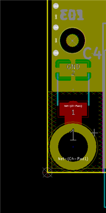
    p.s. for now I tied digital GND and metal enclosure with capacitor over metalized mouning hole. Please look the picture.