Other Parts Discussed in Thread: TL431
Hello,
I am making a new iteration of a power supply with an UCC28740, I can't make it run properly.
Between the last iteration and this one, I'm mainly lowering the max output current from 2.1A to 0.9A.
I use the calculation spreadsheet, and the main difference according to it should the transformer (and the resistors around CS, VS and FB pins).
Samples built of the new transfo have been tested and are in specs with the values of the spreadsheet. Old transfos were made by another company and I'n not sure if they were to spec.
I changed the snubber TVS for an ultrafaster one (Trr went from 500ns to 75ns).
I also added some additional EMI mitigation components (second common mode choke on the AC input to filter radiated noise between 50 and 500MHz) and a ferrite bed in the snubber to remove some of the peaks above 500Mhz.
Both these modifications applied to the old board did not affect functionality, and removing them from this board does not make things better for my problem.
The previous version worked OK (no deviation from expected behaviour that I could detect) after some changes from the calculation sheet made by a TI FAE (larger RLS, adjusted F3/F4 and transformer turn counts IIRC).
Unfortunately I can't say I understood all the details here (he spoke only Chinese), and I can't go back.
VIN: 85 to 245VAC, output 5.6V @ 0.9A
Schematics (I did not show the part making VBLK, it's standard and VBLK is stable.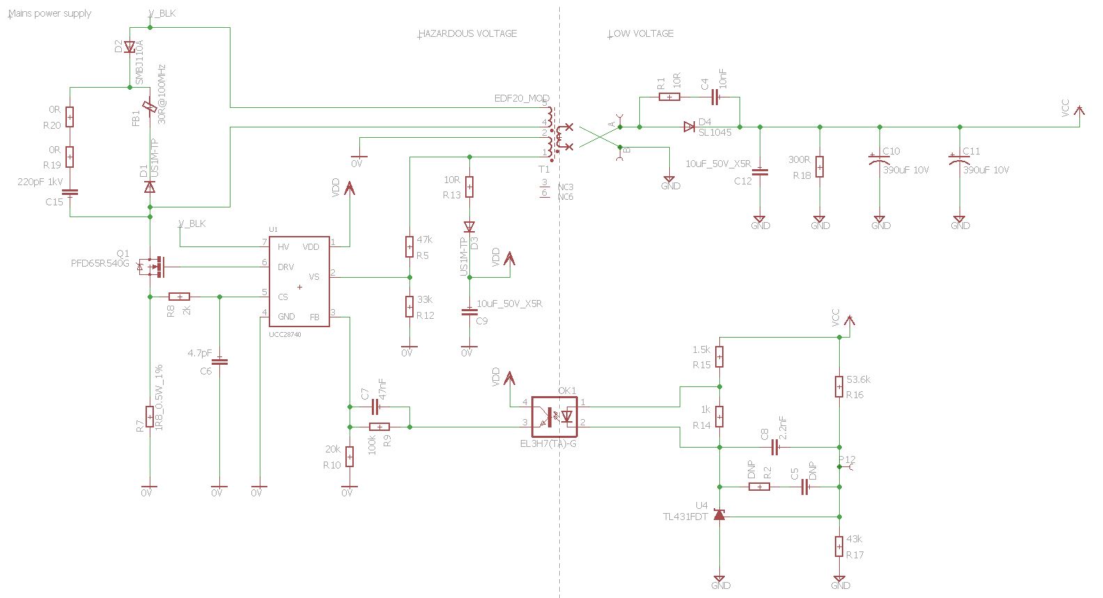
Computation sheet attached.UCC28740 design calculator (5.6V@0.9A).xlsx
With this new version, I have two cases:
1) if I put everything as in the computation sheet (or close to it, cf "actual values"), the chip starts, gets VOUT slightly above VOUT_CV (but below Vout_OVP) then stops.
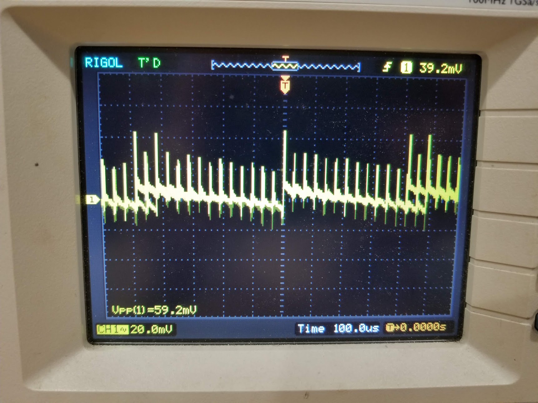
2) if I remove the capacitor CZ (the one between Cathode and REF of the TL431 reference, C8 in my schematics) then the board runs, with a stable output at the right voltage, good behaviour accross loads but the switching pattern is wrong, causing excessive ripple on the ouptut.
In both cases, VBLK is OK, very stable thanks to the slightly oversized bulk caps, and around 300-310V.
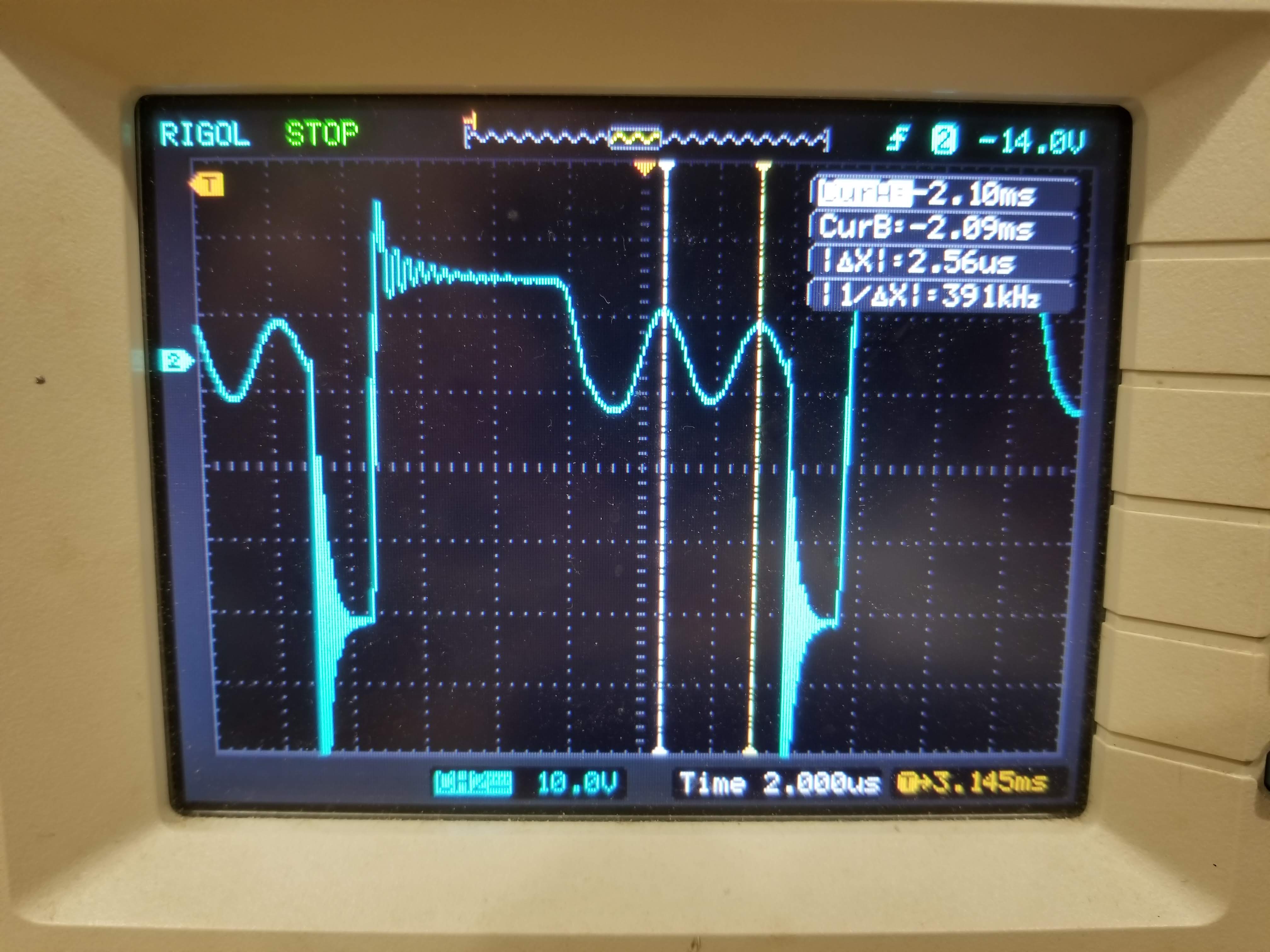
CH2: VAUX. Period of oscillation is 2.56us, larger than expected.
I measured the resonant period, and it seems to be too long: around 2.5us, while Tzto is only 2.1us.
That part is not clear in the datasheet and troubleshooting guide, as it is simply said that the period should be lower than Tzto for fear of missing some of the valley switching - not that it could stop everything from runnning.
I saw a very small number of missed valleys here and there, and if the penalty is only efficiency than I'm OK living with it for now.
Applying the formula for the resonant period (6.1 of "Troubleshooting TI PSR controllers"), knowing the actual inductance of the transformer primary, I get a Csw that, when input in the calculation sheet returns a very different (an shorter) period, so that's a bit misterious here. If that computation was good, then when I changed the MOSFET so that Coss goes from 53pF to 28pF the period should have lowered measurably, but it stayed the same as far as I could tell.
Lowering the inductance would be the opposit of what I'm looking for, and I have no control on the other parameters...
More details on each case:
1)
The chip starts when VDD crosses turnon UVLO threshold, then it switches until the output reaches slightly above the expected output voltage, then it stops switching, seemingly due to CS overvoltage.
VDD goes from 21V to about 14.6V in this time, then slowly drifts down to the turnoff UVLO value before starting another cycle.
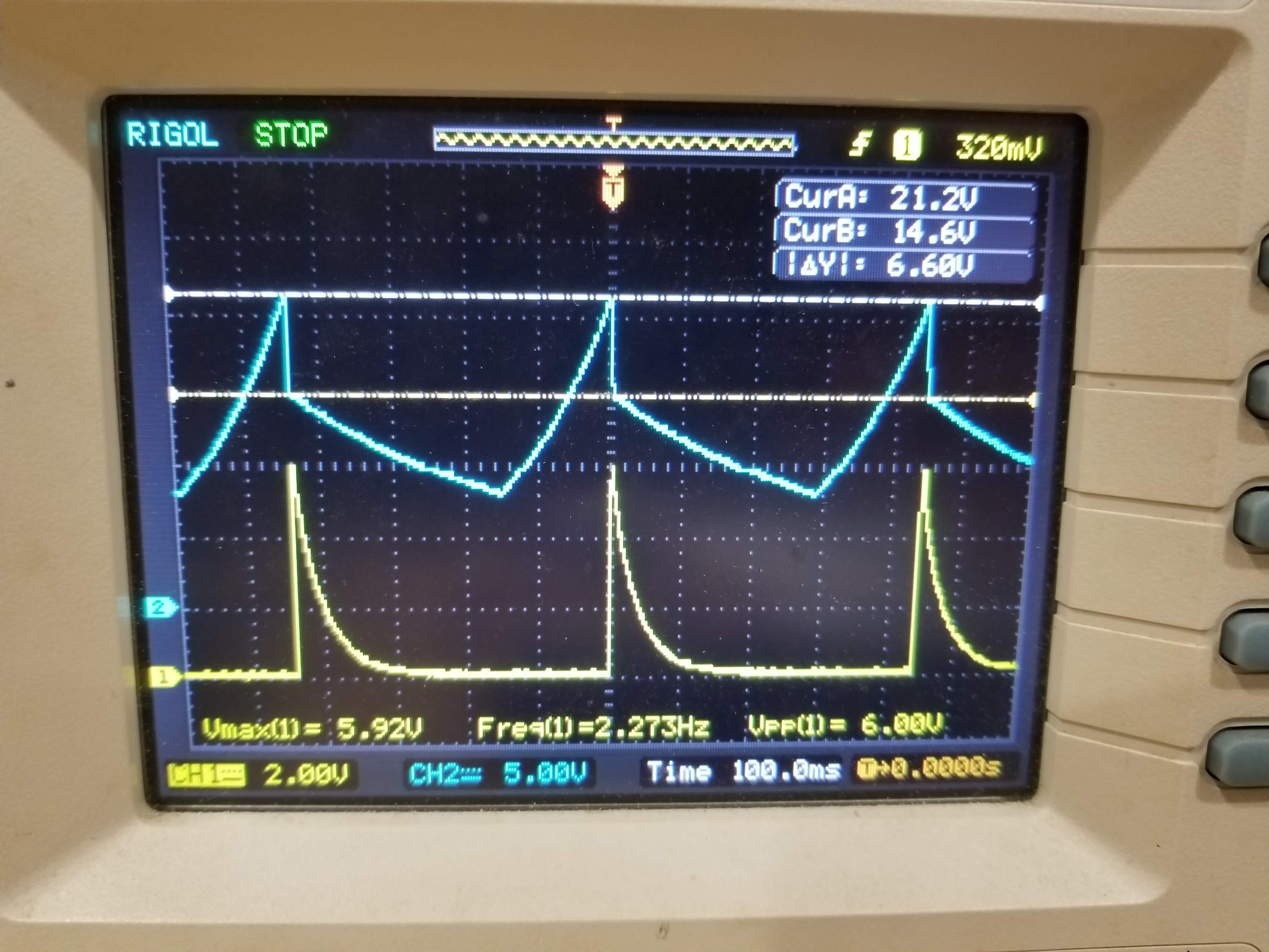
CH1: VOUT, CH2: VDD. Showing multiple cycles. VDD slowly goes down after the chip has stopped switching, until it reaches VDD(off) and restarst the cycle.
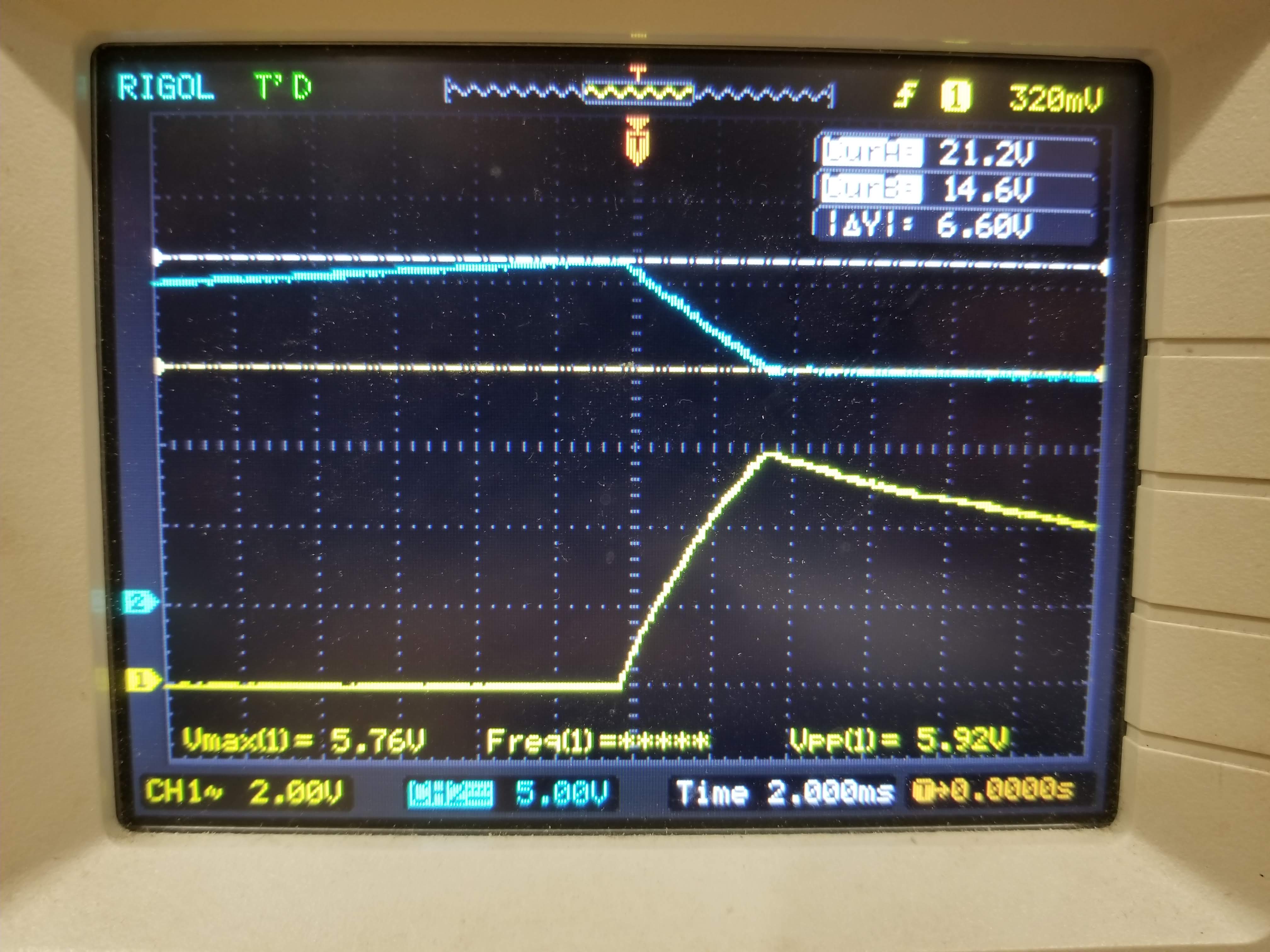
CH1: VOUT, CH2: VDD. Zoomed in on the time during which the chip is running.
Pics of CS, VS and FB during the last cycle(s):
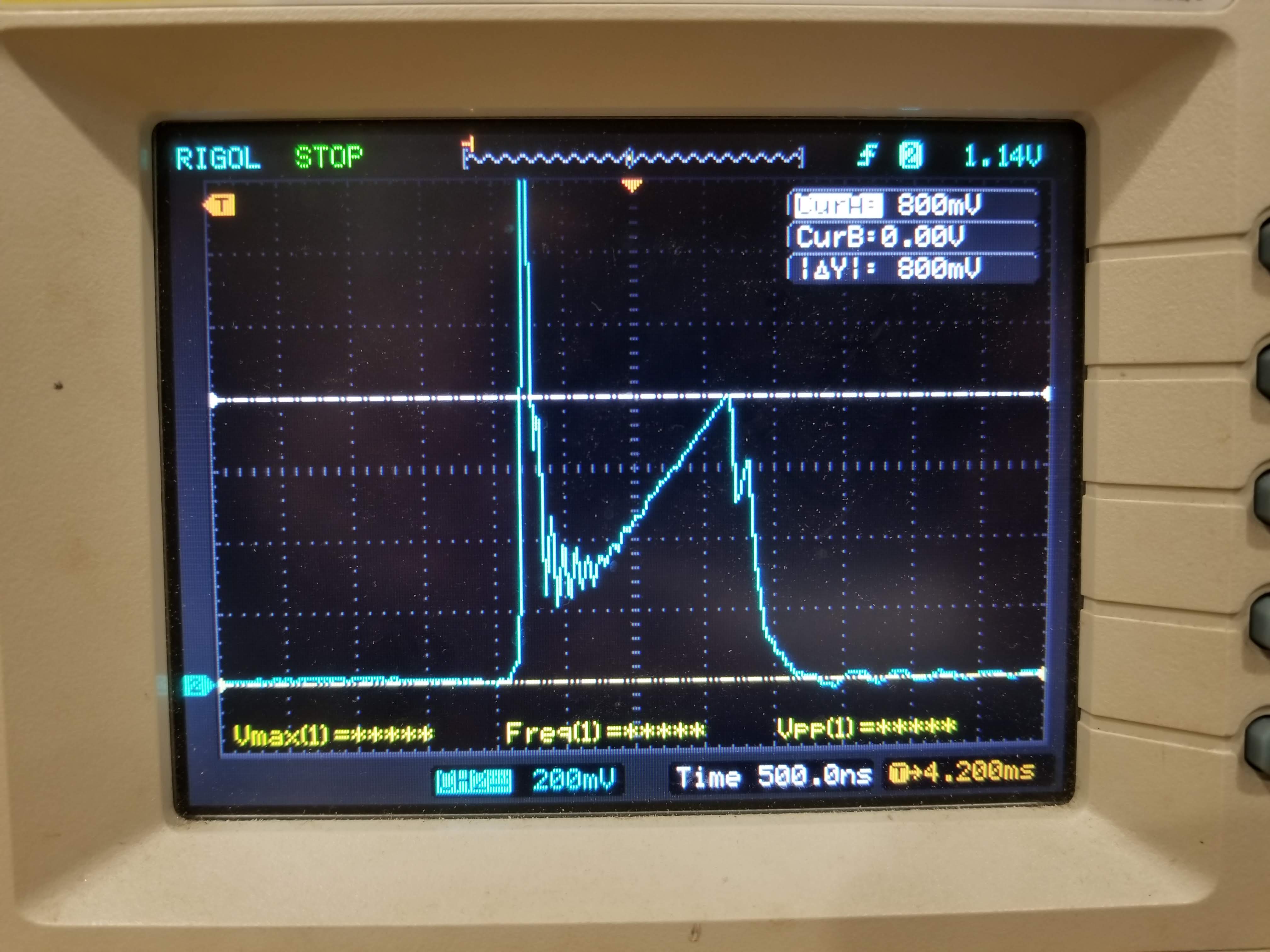
CH2:CS. VCS is above Vcst(max) on the last switching cycle.
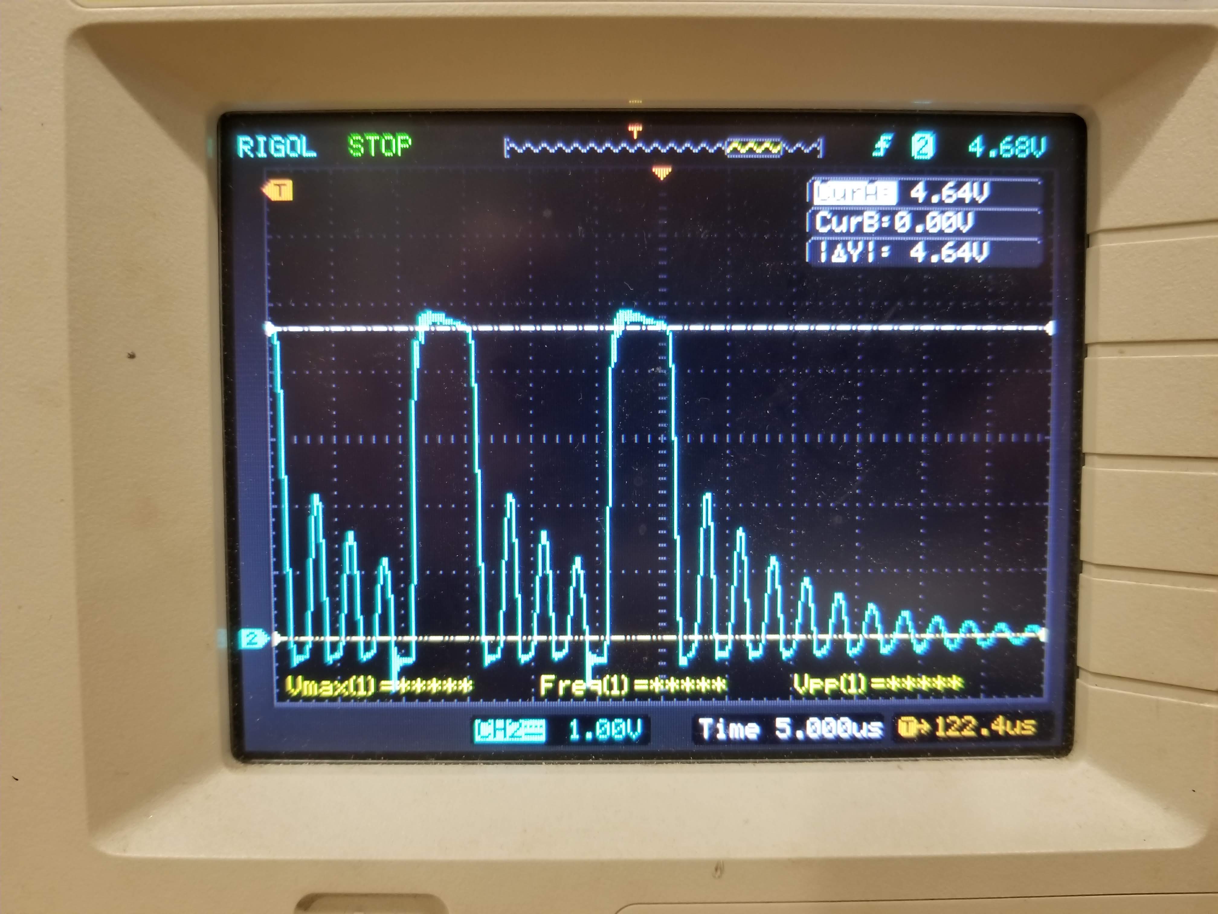
CH2: VS. In the last two cycles, VS goes up to 4.6V.
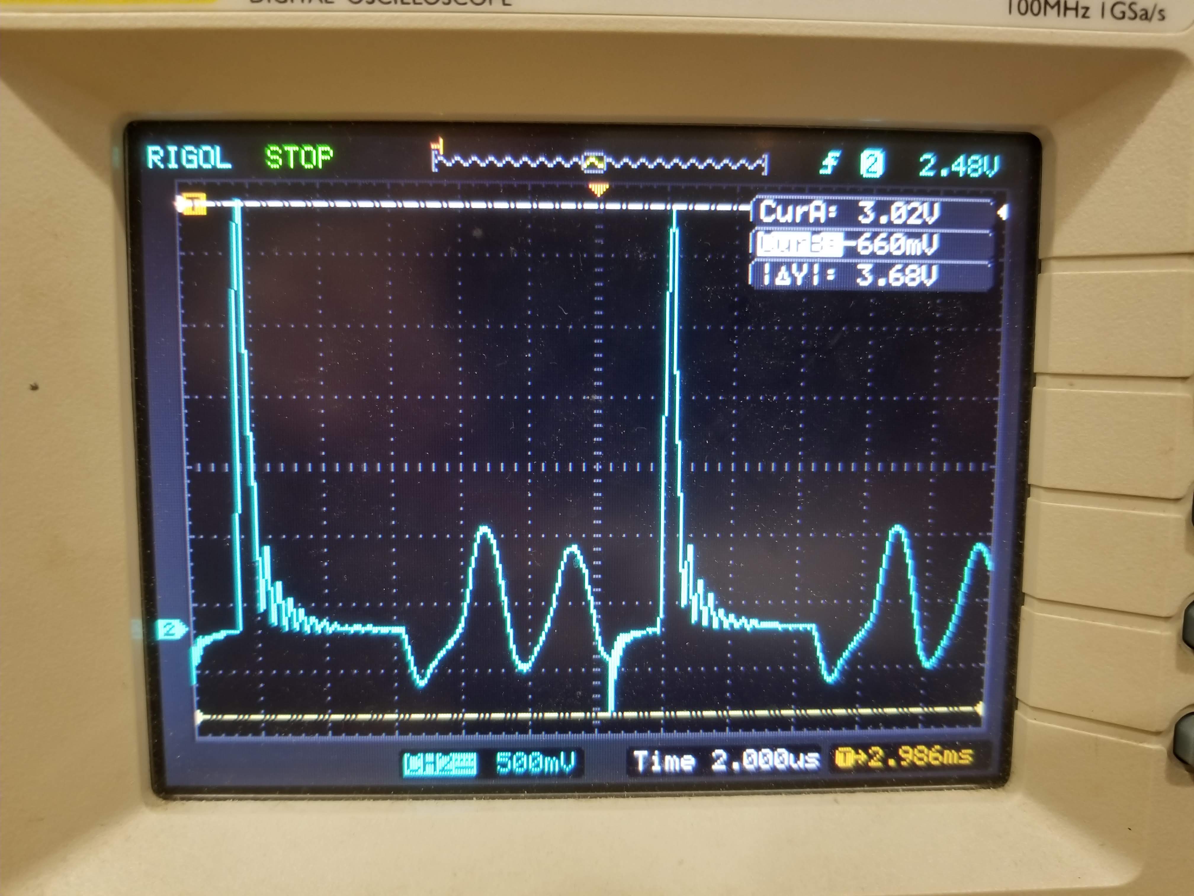
CH2: FB.
If I change RCS and/or RLC to decrease VCS, it will still hit it. I tried with RCS=1.6ohm and RLC=3.3K (instead of 1.8 and 2k), VOUT goes up to 6V before stopping.
2)
In this case, the regulation (when measured RMS) is good, response under load satisfying.
However, the chip works in a kind of burst mode (that is not supposed to exist in this chip). Instead of modulating its frequency to account for load, it will switch at a fixed frequency (around 68 kHz, lower than the theoretical max switching frequency), get the output about 150mV above expected output voltage, then stop until the output goes maybe 200mV under expected output voltage.
The resulting ripple depends on the load, but the switching frequency is the same at no load up to 500mA (I did not test above).
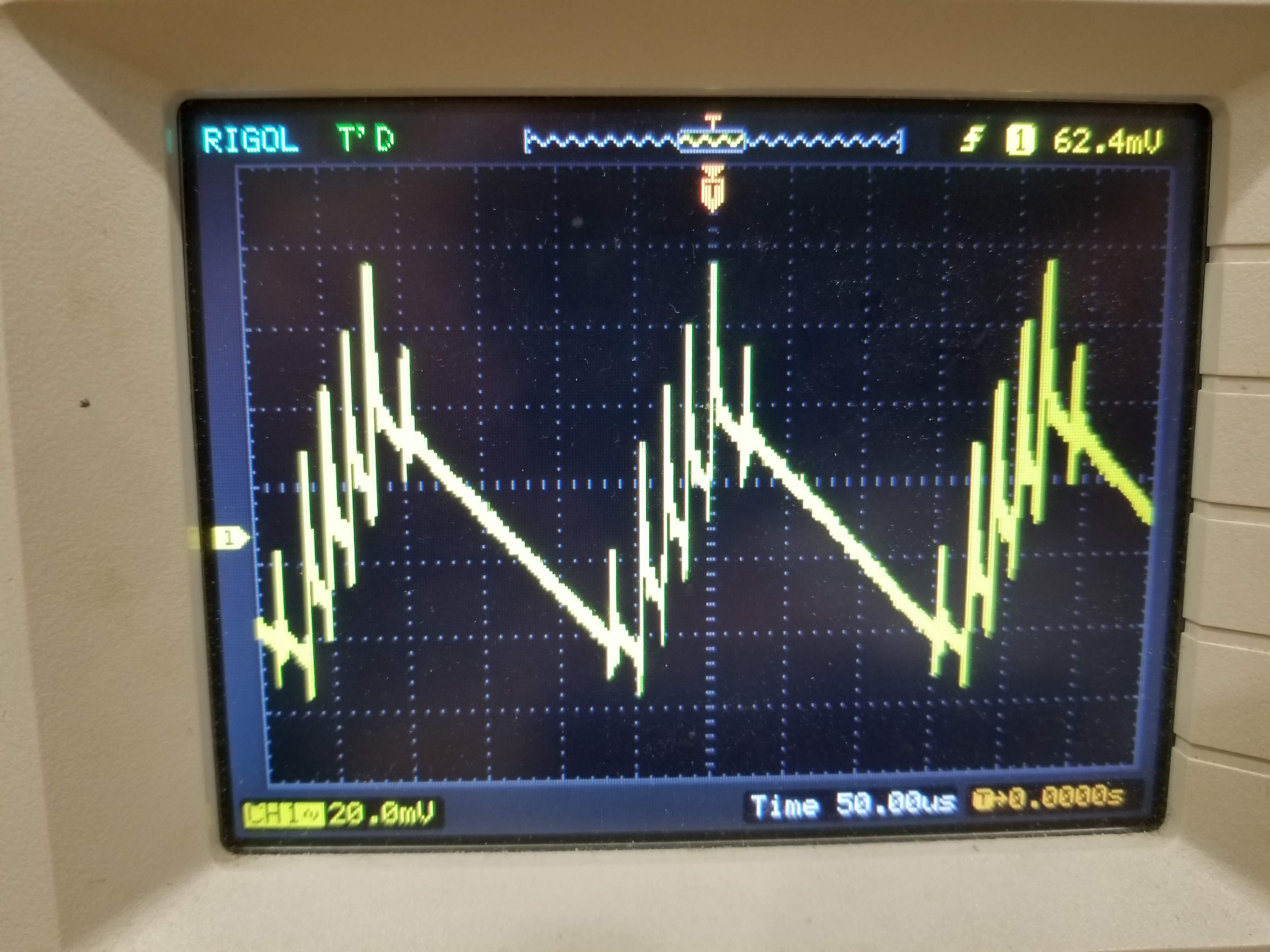
CH1:VOUT. Period is 30us (66.67kHz) when switching. the down slope depends on load, and so does the overall ripple frequency.
I've been working on this for a few days and I'm stumped. There are enough unclear details in the doc (that a seasoned power supply designer probably would not bat an eyelash at) that I'm not sure if I'm making progress or just getting more lost with all the variations in all the resistors I tried...
BTW I have two boards assembled and both behave the same, and as far as I could check all the components are what I think they are (I re-measured all resistors before assembly just in case, I have had Farnell send me wrong values before...)
Any idea what's going on and how to make progress?
Thanks in advance.