Hello,
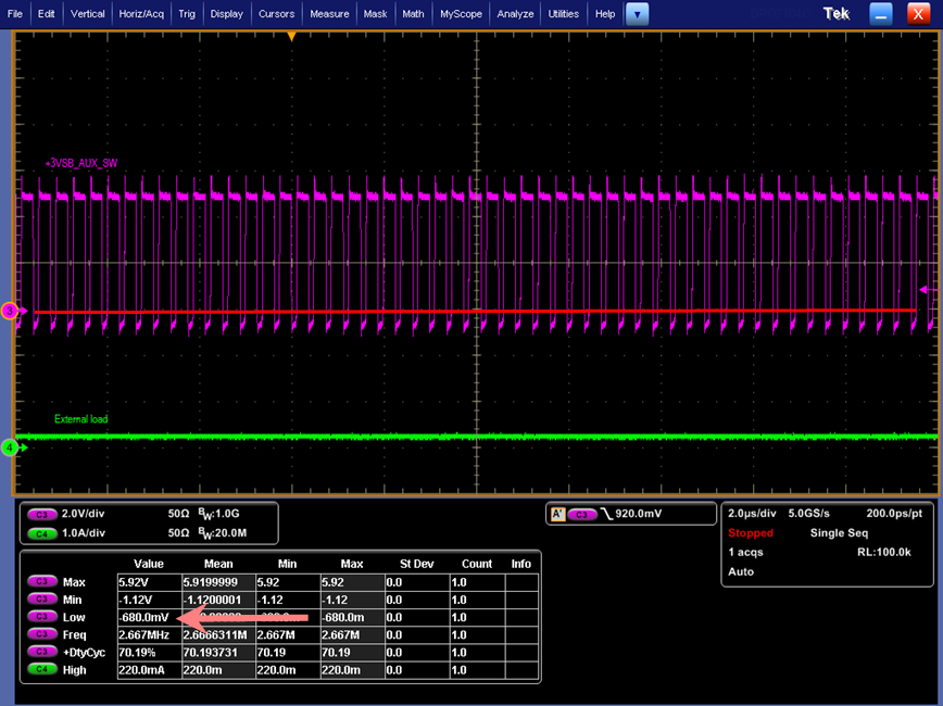
we have observed the phase low level about 0.68V, is it reasonable on PFM operation?
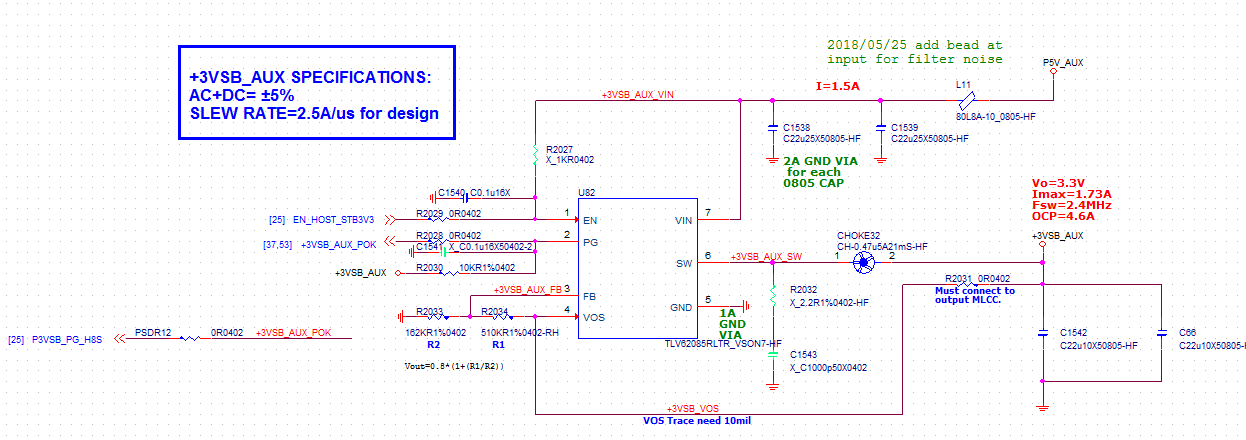
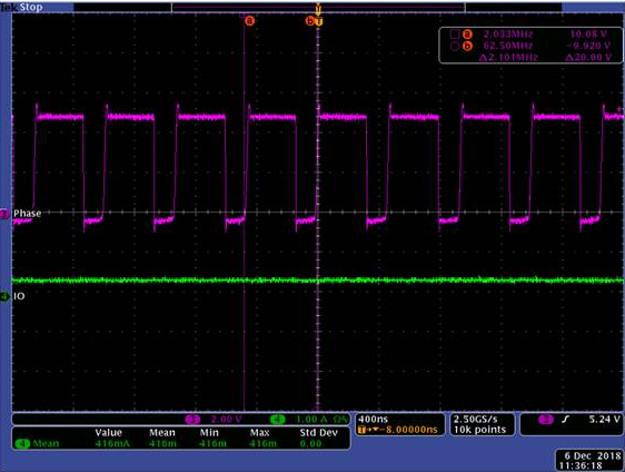
External load=0A
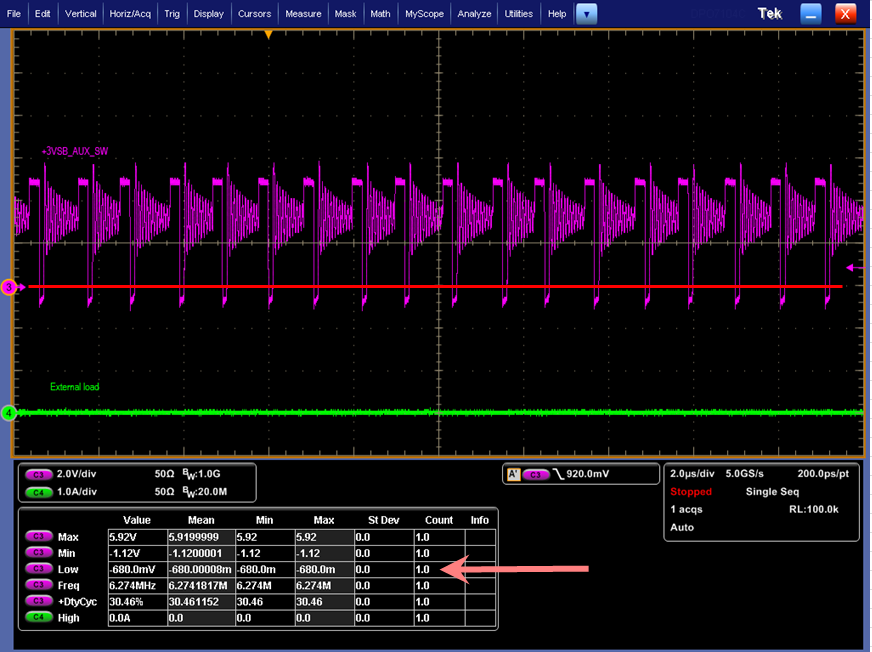
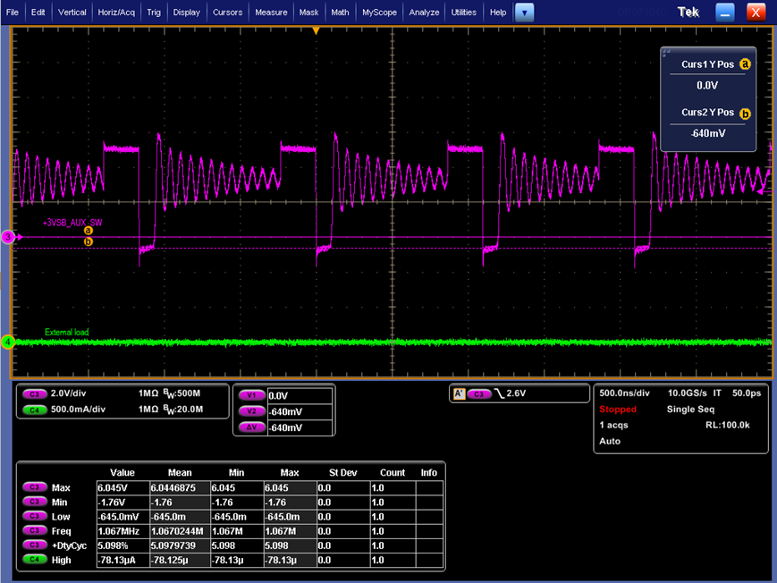
External load=0.22A
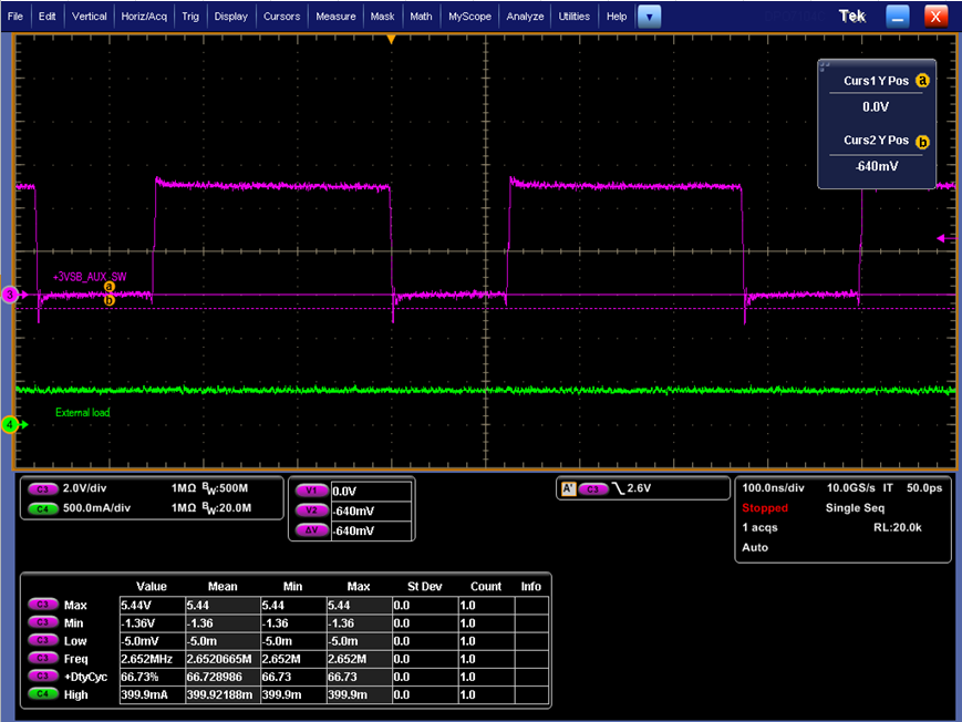
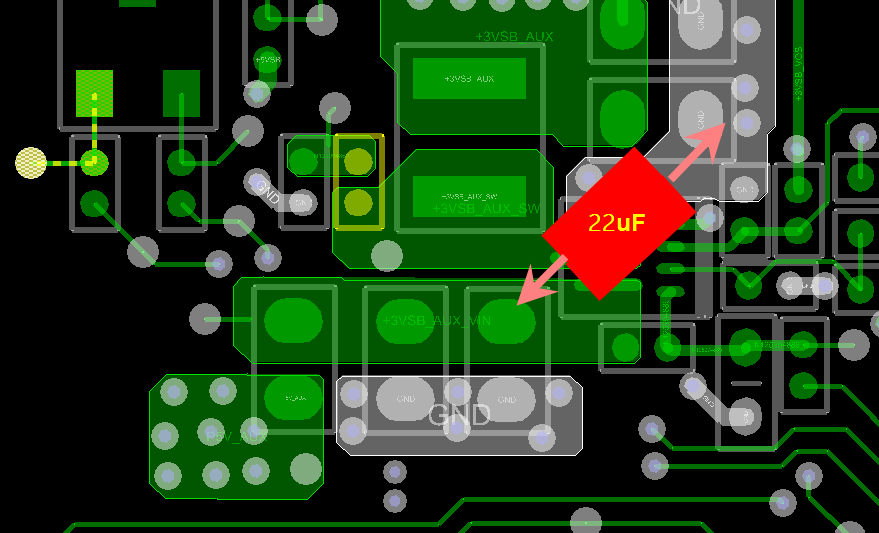
External load=0.4A,負壓消除。
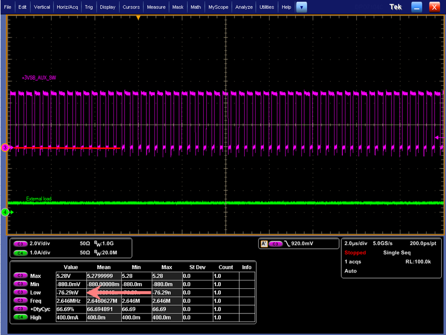
Hello,
we have observed the phase low level about 0.68V, is it reasonable on PFM operation?
External load=0A
External load=0.22A
External load=0.4A,負壓消除。