This thread has been locked.

If you have a related question, please click the "Ask a related question" button in the top right corner. The newly created question will be automatically linked to this question.

LP87702-Q1: Questions regarding the LP87702

Part Number: LP87702-Q1
Other Parts Discussed in Thread: LP87702

Hello Team,

please find below a few questions regarding the LP87702:

1. Looking at the EVB - PMIC schematic it seems like the boost converter is not in use at all. (No net is attached to the PMIC output)

However, it is fully implemented (all the caps and inductor are placed) ... Why is that?

2. Is it possible to order/config PMIC with different I2C addresses? I would them to share the same bus?

3. I am left with a small confusion, in the PMIC datasheet


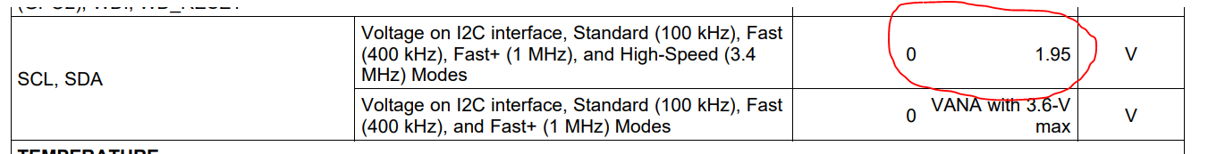
did you mean the 1.95V limitation is only for High-Speed Mode (3.4MHz), Otherwise the limitation is 3.6V, I am correct?

4. as shown at the datasheet there are recommended Operational Conditions for SW_BST are 2.8 - 5.5

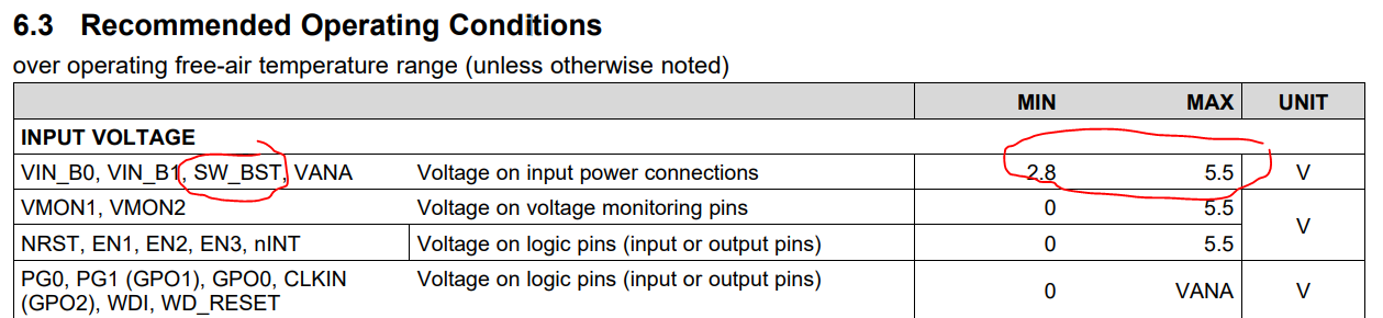
 Later is noted that its input range is 2.8 to 4V (not 5.5V)


Now the Questions:

4A. What is the input range of the boost converter?

4B. In case I don't need it, can it be left floating (input/output) or short it to ground? 

Could you please advise the above, thanks in advance.

Best regards,

Shai

  • Shai,

    Your question has been assigned to our device expert. He should get back to you soon.
  • Hi Shai,

    Apologies for late reply,

    The reason why BOOST external components has been populated is because this LP87702D OTP BOOST is enabled. Without external components device generate PowerGood fault. If we had OTP where the BOOST is disabled, externals are not needed. In that case both BOOST input and output should be connected to GND.

    I2C address can be different, but it needs new partnumber/OTP and it can't be changed via I2C/customer. So it is fixed. If the business case is strong enough, it can be selected as customer wants.

    About the SDA/SCL you have understood correctly. 1.95V limitation is only for High-Speed Mode (3.4MHz)

    BOOST_INPUT pin can handle 2.8-5.5V. But if BOOST is operating mode we are recommend to keep input voltage between 2.8V and 4V. Over 4V BOOST overvoltage protection turn on. LP87702 has also BOOST bypass mode for 5V input, but it is disabled in this OTP. BOOST can be normal or bypass mode, not both. If BOOST bypass mode is selected, BOOST output follow input voltage.

    Tuomo
  • Tuomo, Thank you for your inputs.

    I'll keep you posted in case I got further questions.

    Best regards,

    Shai